Display panel and chip-on-film (COF) package bonding structure, panel bonding pins, package bonding pins, and display panel and cof package bonding method

a chip-on-film and package bonding technology, applied in the direction of printed circuit parts, printed circuit non-printed electric components association, instruments, etc., can solve the problems of excessive expansion or insufficient expansion, failure of the bonding process, etc., and achieve the effect of improving the bonding ra

Active Publication Date: 2021-07-08
WUHAN CHINA STAR OPTOELECTRONICS SEMICON DISPLAY TECH CO LTD
View PDF0 Cites 0 Cited by
  • Summary
  • Abstract
  • Description
  • Claims
  • Application Information

AI Technical Summary

Benefits of technology

[0005]The main objective of the present invention is to provide a display panel and chip-on-film (COF) package bonding structure, panel bonding pins, package bonding pins, and a display panel and COF package bonding method. When excessive or insufficient expansion of the COF occurs during bonding of the display panel and the COF package, the display panel and COF package bonding structure can by shifting the COF bond bonding pins of the COF accurately to bonding pins of display panel such that bonding rate is improved.

Problems solved by technology

Even though the pins of the COF package are designed to be narrowed and closer under consideration of expansion factor of the COF package during the bonding process, the COF package may still excessively expand or insufficiently expand during the bonding process and causes the COF package not bonded correctly to the display panel and results in failure of the bonding process.

Method used


Image

  • Display panel and chip-on-film (COF) package bonding structure, panel bonding pins, package bonding pins, and display panel and cof package bonding method
  • Display panel and chip-on-film (COF) package bonding structure, panel bonding pins, package bonding pins, and display panel and cof package bonding method
  • Display panel and chip-on-film (COF) package bonding structure, panel bonding pins, package bonding pins, and display panel and cof package bonding method

Examples


Embodiment Construction

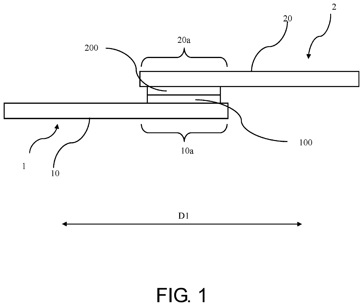
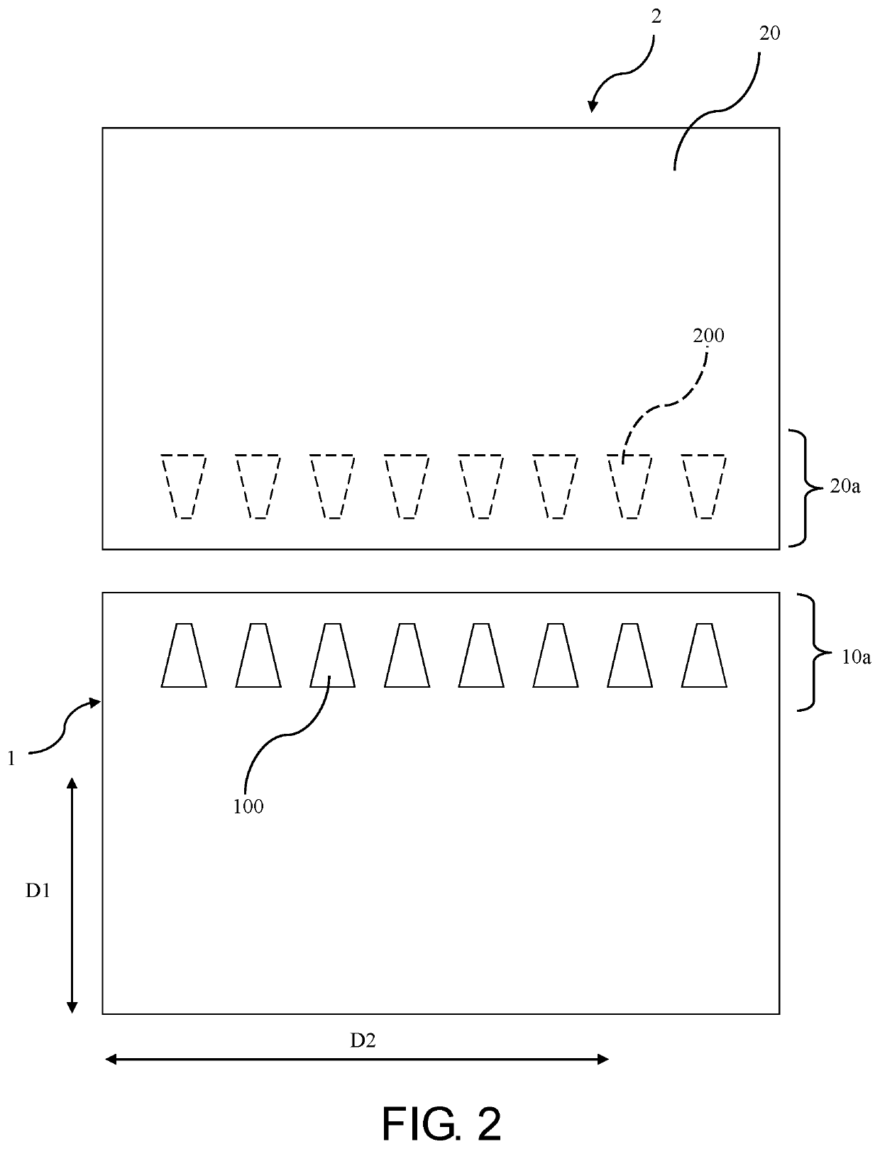
[0042]With reference to FIGS. 1 and 2, a bonding structure of a display panel and a chip-on-film (COF) package includes: a display panel 1 and a COF package 2.

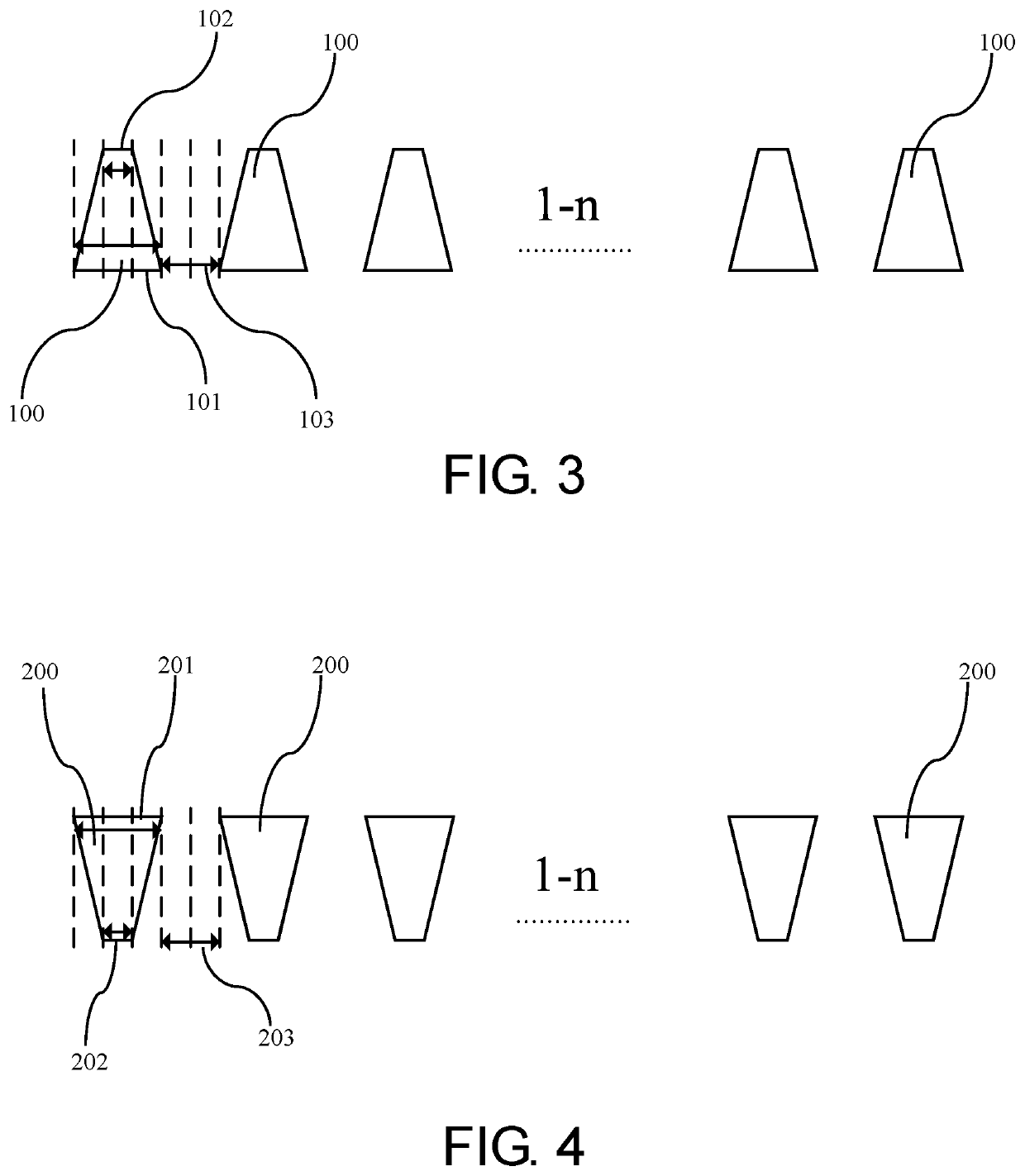
[0043]With reference to FIG. 3, the display panel 1 include a panel substrate 10 and a plurality of panel bonding pins 100.

[0044]A panel bonding portion 10a is formed on an end of the panel substrate 10. The panel bonding pins 100 are disposed on the panel bonding portion 10a and are arranged along a lateral direction D2 of the panel bonding portion 10a. “1−n” shown in FIG. 3 means that a number of the panel bonding pins 100 is n. Each of the panel bonding pins 100 is trapezoidal, is directed along a longitudinal direction D1 of the panel bonding portion 10a, is tapered forward (tapered toward the COF package 2), and includes a wide rear end portion 101 and a narrow front end portion 102 opposite to the wide rear end portion 101. Furthermore, a width of the wide rear end portion 101 is three times a width of the narrow front e...


PUM

PropertyMeasurementUnit
bonding structureaaaaaaaaaa
widthaaaaaaaaaa
sizeaaaaaaaaaa

Abstract

A display panel and chip-on-film (COF) package bonding structure is provided and includes a display panel including a panel substrate and a plurality of panel bonding pins. The panel bonding pins are disposed on the panel substrate and are arranged along a lateral direction. Each of the panel bonding pins is trapezoidal and is directed along a longitudinal direction. A COF package is bonded to the display panel and includes a package substrate and a plurality of package bonding pins. The package bonding pins are disposed on the package substrate, are arranged along the lateral direction, and are bonded to the panel bonding pins respectively. Each of the package bonding pins is trapezoidal and along the longitudinal direction. The trapezoidal panel bonding pins and package bonding pins can be aligned with and contacts each other.

Description

FIELD OF INVENTION[0001]The present invention relates to a bonding structure, especially to a display panel and chip-on-film (COF) package bonding structure, panel bonding pins, package bonding pins, and a display panel and COF package bonding method. When excessive or insufficient expansion of the COF occurs during bonding of the display panel and the COF package, the display panel and COF package bonding structure can by shifting the COF bond bonding pins of the COF accurately to bonding pins of display panel such that bonding rate is improved.BACKGROUND OF INVENTION[0002]At present, demands for full screen displays in the markets becomes greater. Design of screen-to-body ratio for full screen displays is required to reduce an area of an outer lead bonding (OLB) region of a display panel as possible. To reduce the area of the OLB region, it becomes popular to bond an integrated circuits (IC) chip to a chip-on film (COF) package such that the COF package can be bonded to a display ...

Claims


Application Information

Patent Timeline
Patent Type & Authority Applications(United States)
IPC IPC(8): H05K1/18G06F1/18
CPCH05K1/181H05K2201/10318H05K2201/10128G06F1/189H10K50/84H10K71/00G06F1/1658G06F1/1626
Inventor TONG, PEIQIAN
Owner WUHAN CHINA STAR OPTOELECTRONICS SEMICON DISPLAY TECH CO LTD
Why Eureka
Try Eureka