Light-irradiation heat treatment apparatus
a heat treatment apparatus and light-irradiation technology, applied in lighting and heating apparatus, electric heating for furnaces, furnaces, etc., can solve the problems of insufficient level of uniform temperature distribution, hinder the formation of good devices, and the junction depth may become too deep, so as to achieve the effect of increasing directivity
- Summary
- Abstract
- Description
- Claims
- Application Information
AI Technical Summary
Benefits of technology
Problems solved by technology
Method used
Image

Examples
first preferred embodiment
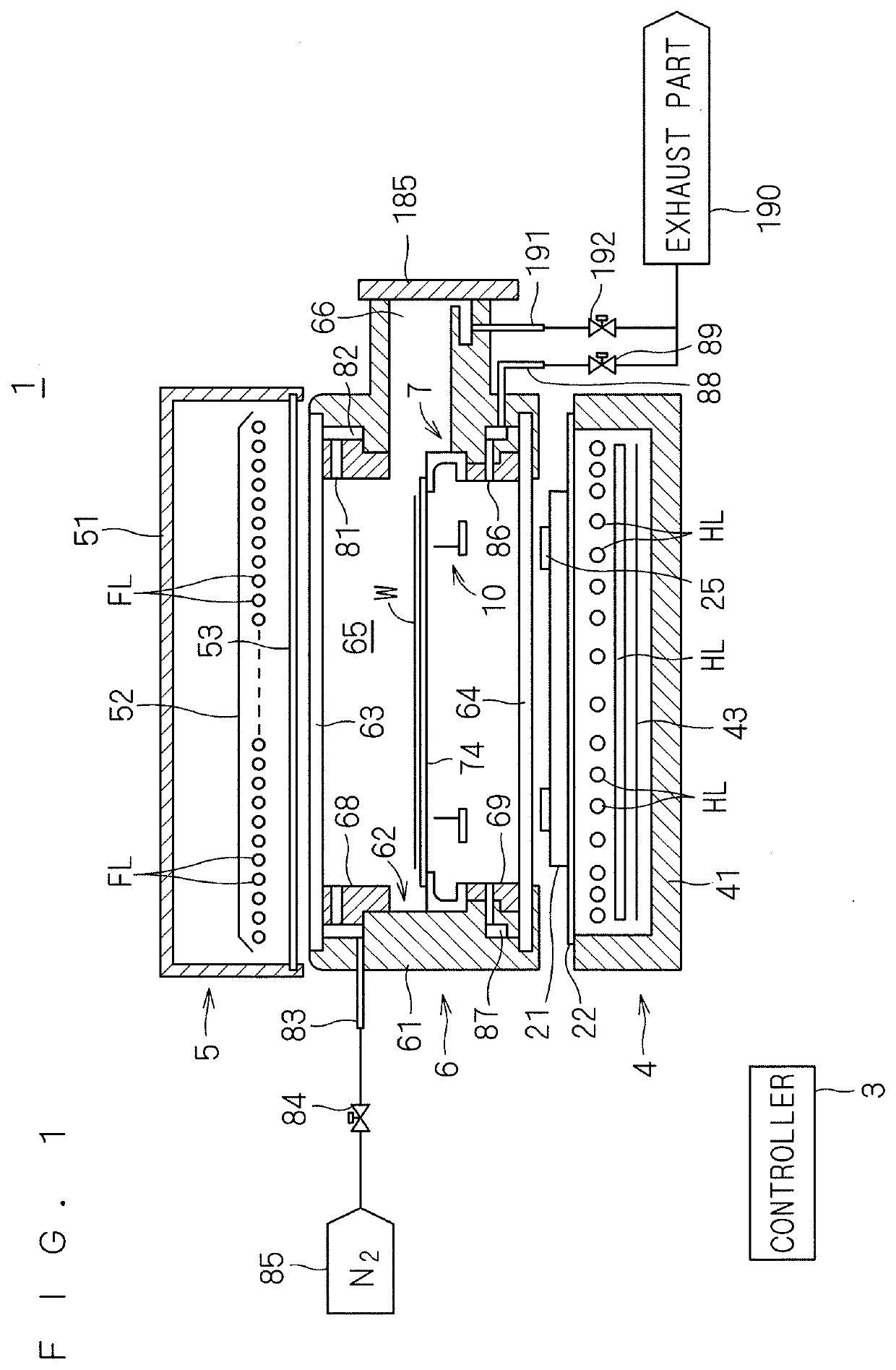
[0042]FIG. 1 is a longitudinal cross-sectional view of a configuration of a heat treatment apparatus 1 according to the present invention. The heat treatment apparatus 1 of the present preferred embodiment is a flash-lamp annealing apparatus for heating a disk-shaped semiconductor wafer W having a diameter of 300 mm as a substrate by irradiating the semiconductor wafer W with flash light. The semiconductor wafer W is doped with impurities before being transported into the heat treatment apparatus 1, and the doped impurities are activated through heat treatment by the heat treatment apparatus 1. For easy understanding of drawings, the dimensions and number of each constituent element may be exaggerated or simplified as necessary in FIG. 1 and subsequent drawings.
[0043]The heat treatment apparatus 1 includes a chamber 6 that houses the semiconductor wafer W, a flash heating part 5 with a plurality of built-in flash lamps FL, and a halogen heating part 4 with a plurality of built-in ha...
second preferred embodiment
[0097]Next, a second preferred embodiment according to the present invention will be described. The overall configuration of a heat treatment apparatus of the second preferred embodiment is approximately the same as the configuration of the first preferred embodiment. The procedure of processing performed on the semiconductor wafer W in the second preferred embodiment is also the same as the procedure in the first preferred embodiment. The second preferred embodiment is different from the first preferred embodiment in the shape of a light-shielding member.
[0098]FIG. 11 is a plan view of a light-shielding member 125 of the second preferred embodiment. While the light-shielding member 25 of the first preferred embodiment is an annular flat plate-like light-shielding ring, the light-shielding member 125 of the second preferred embodiment is a square plate-like member having a square hole in the center. The light-shielding member 125 of the second preferred embodiment can also be called...
third preferred embodiment
[0102]Next, a third preferred embodiment of the present invention will be described. The overall configuration of a heat treatment apparatus of the third preferred embodiment is approximately the same as the configuration of the first preferred embodiment. The procedure of processing performed on the semiconductor wafer W in the third preferred embodiment is also the same as the procedure of the first preferred embodiment. The third preferred embodiment is different from the first preferred embodiment in the shape of a light-shielding member.
[0103]FIG. 12 is a plan view of a light-shielding member 225 of the third preferred embodiment. The light-shielding member 225 of the third preferred embodiment is configured by a plurality of light-shielding parts, with four plate-like light-shielding pieces 222 being located inward of an annular flat plate-like light-shielding ring 221. The light-shielding ring 221 and the four light-shielding pieces 222, which constitute the light-shielding m...
PUM
| Property | Measurement | Unit |
|---|---|---|
| diameter | aaaaa | aaaaa |
| inner diameter | aaaaa | aaaaa |
| inner diameter | aaaaa | aaaaa |
Abstract
Description
Claims
Application Information
 - R&D
- Intellectual Property
- Life Sciences
- Materials
- Tech Scout
- Unparalleled Data Quality
- Higher Quality Content
- 60% Fewer Hallucinations
Browse by: Latest US Patents, China's latest patents, Technical Efficacy Thesaurus, Application Domain, Technology Topic, Popular Technical Reports.
© 2025 PatSnap. All rights reserved.Legal|Privacy policy|Modern Slavery Act Transparency Statement|Sitemap|About US| Contact US: help@patsnap.com