Three-dimensional stacked phase change memory and preparation method thereof

a phase change memory and three-dimensional technology, applied in the field of microelectronic devices and memories, can solve the problems of limited memory cell feature size, low reliability, photoetching process, etc., and achieve the effect of reducing the number of photoetching operations, increasing the cost of the photoetching process, and reducing the number of times of photoetching operations

Active Publication Date: 2021-09-09
HUAZHONG UNIV OF SCI & TECH
View PDF0 Cites 1 Cited by
  • Summary
  • Abstract
  • Description
  • Claims
  • Application Information

AI Technical Summary

Benefits of technology

[0028]By comparing the above technical solution of the present inventive concept with the prior art, the present disclosure has the following beneficial effects. The existing 3D XPoint memory mainly adopts a planar three-dimensional stacking manner, in which a lower electrode (word line), an insulating layer, a selector layer, a phase change memory layer, an upper electrode (bit line) and so on are deposited layer by layer, and then the above steps are repeated to realize multi-layer stacking. The method adopts the existing preparation method of the planar phase change memory, in which the selector and the phase change memory can be integrated by simple continuous deposition. However, the number of times of photoetching operations is proportional to the number of the three-dimensional stacked layers, the cost of the photoetching process is increased sharply during the multi-layer stacking, and the preparation of each layer of electrodes causes a certain surface unevenness, leading to the serious device reliability problem in multi-layer stacking. Although a 3D XPoint memory based on vertical electrode is mentioned some materials (such as the master's thesis in the present research group “research on preparation process of 3D XPoint memory”), only a simple electrode structure diagram is provided, without disclosing the structural design and process implementation of the specific layers of the 3D XPoint memory and even considering the selectors required by the actual 3D XPoint memory. In the present disclosure, the size design of respective layers, the implementation of overlay, and the effective integration of the selectors and the storage units are the difficulties of the vertical three-dimensional stacking method compared with the horizontal stacking method. Compared with the existing 3D XPoint memory based on horizontal electrode structure, the present disclosure adopts a vertical electrode structure, in which all bit lines are deposited once by etched vias, which greatly reduces the number of times of photoetching operations during multi-layer stacking, and thus effectively reducing the cost; and in the preparation process, each functional material is almost contoured in the plane, and the excess material can be removed by etching, effectively alleviating the surface irregularity caused by multilayer stacking. In addition, the feature size of the memory cell according to the present disclosure is determined by the film thickness, not the processing line width, which increases the storage density to establish a large-capacity three-dimensional memory array, and reduces the phase change region size (as low as 2 nm) to reduce the operating current and the power consumption.
[0029]In summary, the present disclosure adopts a cross structure of a horizontal electrode and a vertical electrode to realize multi-layer stacking in a vertical direction. The phase change units have a small feature size and a relatively flat surface, which is advantageous for stacking more layers and reducing the operating current and the power consumption.

Problems solved by technology

Although this structure is simple, with the increase of the number of stacked layers, the process steps are cumbersome, and the surface unevenness is intensified, bringing about the reliability problem.
In addition, the feature size of the memory cell is limited by advanced photoetching processes, which are costly.
Overall, it is not conducive to further multi-layer stacking and high-density integration.
However, the number of times of photoetching operations is proportional to the number of the three-dimensional stacked layers, the cost of the photoetching process is increased sharply during the multi-layer stacking, and the preparation of each layer of electrodes causes a certain surface unevenness, leading to the serious device reliability problem in multi-layer stacking.

Method used


Image

  • Three-dimensional stacked phase change memory and preparation method thereof
  • Three-dimensional stacked phase change memory and preparation method thereof
  • Three-dimensional stacked phase change memory and preparation method thereof

Examples


embodiment 1

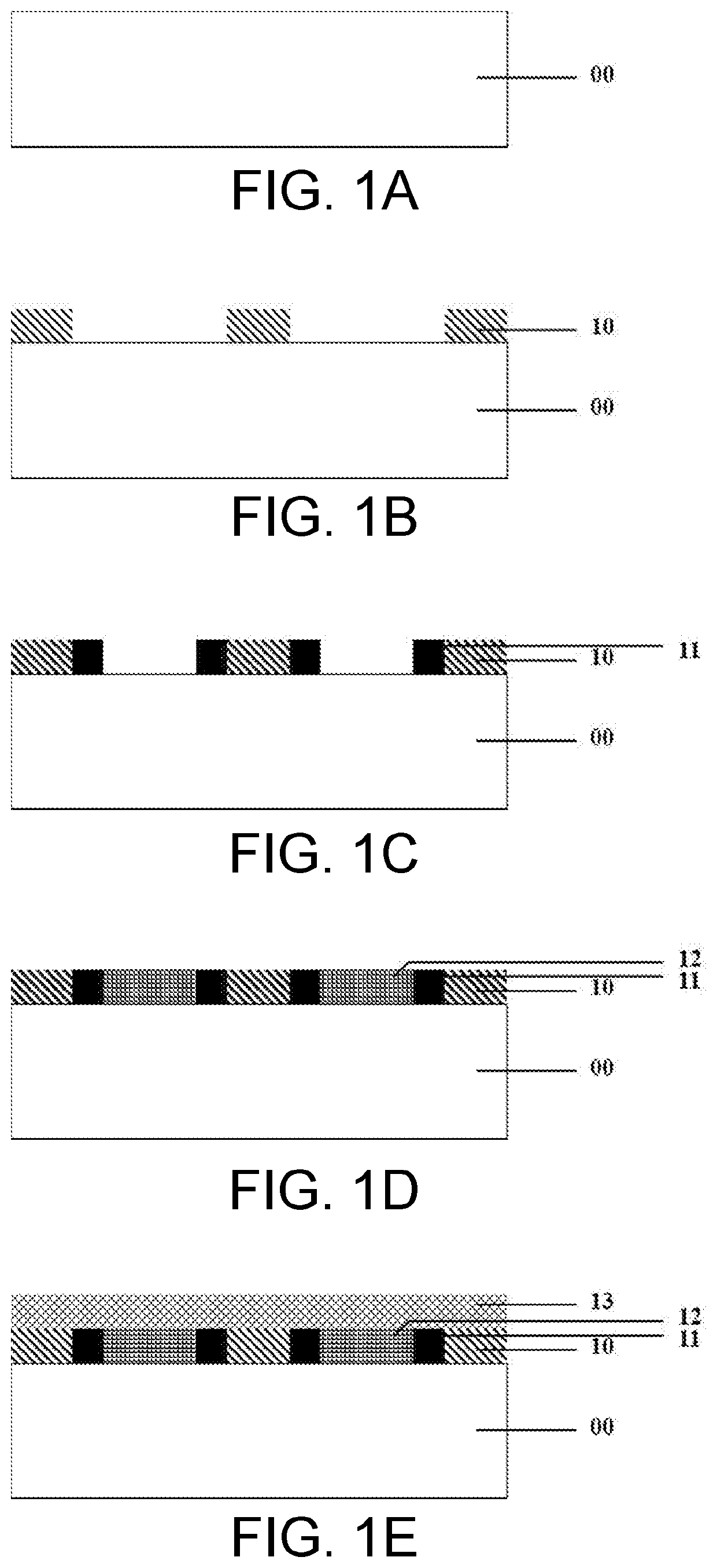
[0071]In this embodiment, a three-dimensional stacked phase change memory and a preparation method thereof are provided by taking a multilayer stacked memory as an example, and the method specifically includes the following steps.

[0072]Step 1: performing a photoetching process on a single crystal silicon substrate 00 to obtain a plurality of first horizontal electrode patterns having a line width of 10 μm and an interval of 15 μm in a certain direction, depositing a 100 nm TiW alloy electrode material on the photoetched substrate, and then performing a lift-off process to obtain first horizontal electrodes 10 corresponding to the photoetching patterns, as shown in FIG. 1A to FIG. 1B and FIG. 2A to FIG. 2B.

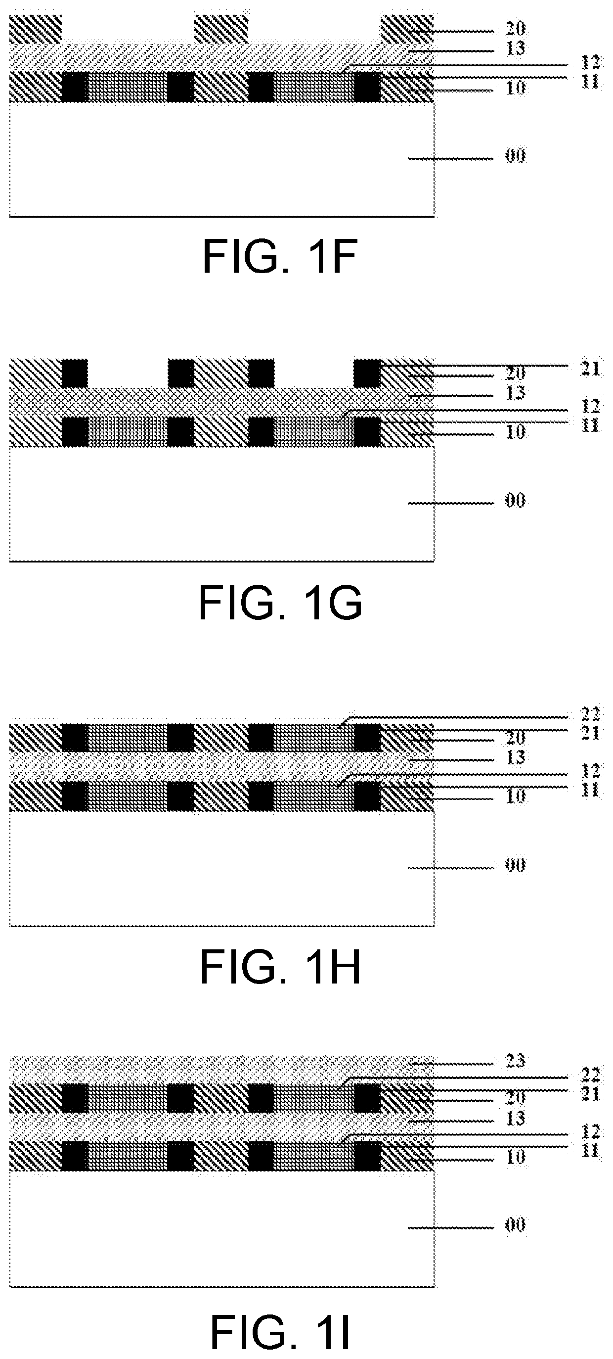
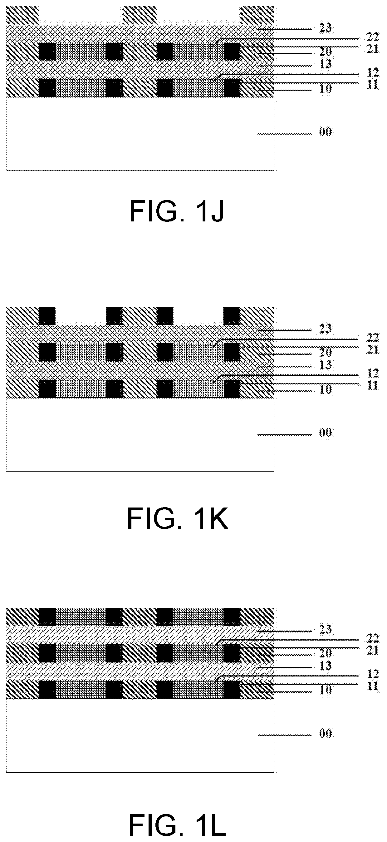
[0073]Step 2: on the basis of the step 1, performing a photoetching process to obtain first strip-shaped phase change layer patterns having a line width of 17 μm, a central gap of 10 μm and an interval of 8 μm, in which the patterns cover the intervals of the first horizontal elect...


PUM

PropertyMeasurementUnit
widthaaaaaaaaaa
widthaaaaaaaaaa
widthaaaaaaaaaa

Abstract

A three-dimensional stacked phase change memory and a preparation method thereof are provided. The method comprises: preparing first horizontal electrodes spaced apart from each other on a substrate; preparing first strip-shaped phase change layers, each having a central gap, between the first horizontal electrodes; preparing first selectors in the central gaps of the first strip-shaped phase change layers; preparing a first insulating layer; preparing second strip-shaped phase change layers at same vertical positions on the first insulating layer; preparing second selectors; then preparing horizontally-oriented insulating holes between the horizontal electrodes; and preparing vertical electrodes between the adjacent insulating holes, thereby forming a multilayer stacked phase change memory with a vertical structure.

Description

CROSS-REFERENCE TO RELATED APPLICATION[0001]This application is a 371 application of the International PCT application serial no. PCT / CN2018 / 118146, filed on Nov. 29, 2018, which claims the priority benefit of China application no. 2018110847703, filed on Sep. 18, 2018. The entirety of each of the above-mentioned patent applications is hereby incorporated by reference herein and made a part of this specification.BACKGROUNDTechnical Field[0002]The disclosure belongs to the technical field of microelectronic devices and memories, and more particularly relates to a three-dimensional stacked phase change memory and a preparation method thereof.Description of the Related Art[0003]As a new type of memory that is most likely to become one of the mainstream memories in the future, the phase change memory has gradually evolved into three dimensions to meet the demand for high-capacity storage in the era of big data, forming a multi-layer stacked phase change memory.[0004]At present, the thre...

Claims


Application Information

Patent Timeline
Patent Type & Authority Applications(United States)
IPC IPC(8): H01L45/00H01L27/24
CPCH01L45/1683H01L27/249H01L45/1675H01L45/1253H01L45/1608H01L45/06H10B63/84H10N70/011H10N70/021H10N70/8828H10B63/845H10N70/066H10N70/063H10N70/231H10N70/841
Inventor MIAO, XIANGSHUITONG, HAOSHEN, YUSHANCAI, WANG
Owner HUAZHONG UNIV OF SCI & TECH
Why Eureka
Try Eureka