
Power amplifier circuit

a power amplifier and circuit technology, applied in amplifiers, amplifier protection circuit arrangements, amplifiers with semiconductor devices/discharge tubes, etc., can solve the problems of reflected waves and increase the loss of power amplifier circuits

Pending Publication Date: 2021-09-30
MURATA MFG CO LTD
View PDF6 Cites 1 Cited by
  • Summary
  • Abstract
  • Description
  • Claims
  • Application Information

AI Technical Summary

Benefits of technology

The technical effect of this patent is to reduce the impact of reflected waves and minimize the increase in power caused by changes in the load.

Problems solved by technology

In recent years, because the load loss of a power amplifier circuit increases as a front-end circuit configuration is complicated, the power amplifier circuit has been required to output higher power.
In the power amplifier circuit described in the above-mentioned Patent Document, however, because clamp diodes are connected in output matching and an RF signal is detected from an anode of a predetermined diode among the clamp diodes, it has no directivity, and thus it may be affected by reflected waves.

Method used


Image

  • Power amplifier circuit
  • Power amplifier circuit
  • Power amplifier circuit

Examples


Embodiment Construction

[0020]Embodiments of the present disclosure are described below with reference to the drawings. Here, circuit elements of the same reference numerals indicate the same circuit elements, and the overlapping description is omitted.

===Configuration of Power Amplification Module 1===

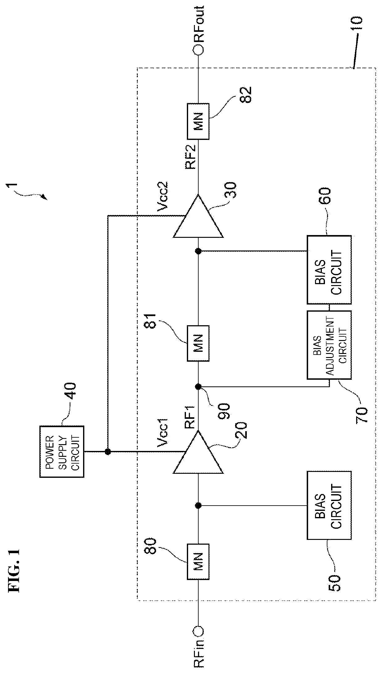
[0021]FIG. 1 schematically illustrates a configuration of a power amplification module 1 including a power amplifier circuit 10 according to an embodiment. One example of the power amplification module 1 may be mounted on a mobile communication device, such as a cellular phone, amplify the power of an input signal RFin to a level required to be transmitted to a base station, and output the resultant signal as an amplified signal RFout. One example of the input signal RFin may be a radio frequency (RF) signal modulated by a radio frequency integrated circuit (RFIC) or the like in accordance with a predetermined communication scheme. Examples of the communication standard for the input signal RFin may include ...


PUM


Abstract

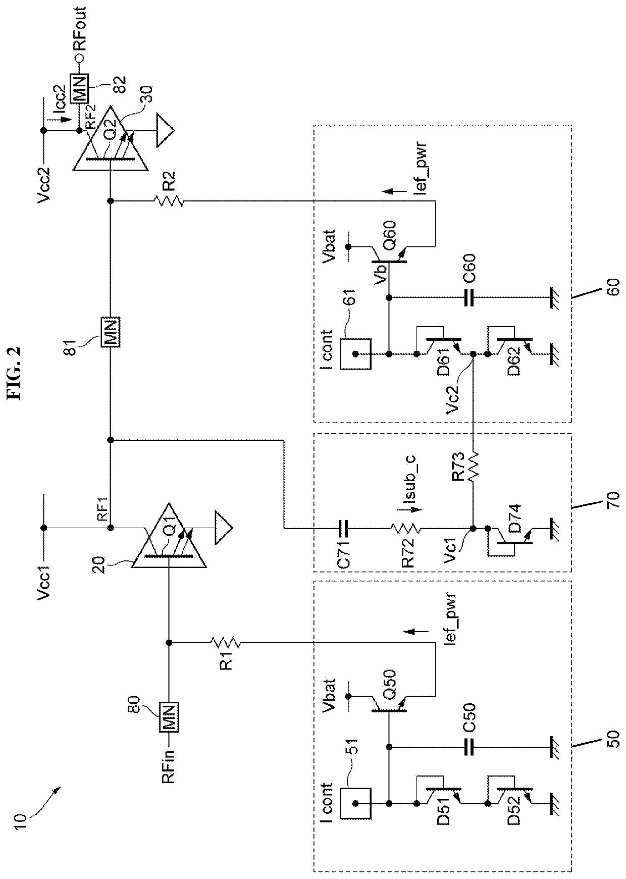
A power amplifier circuit includes a first amplifier that amplifies a first RF signal and outputs a second RF signal, a second amplifier that amplifies the second RF signal and outputs a third RF signal, a bias circuit that supplies a bias current or voltage to the first or second amplifier, and a bias adjustment circuit that adjusts the bias current or voltage on the basis of the first RF signal, the second RF signal, or the third RF signal. The bias adjustment circuit includes a first diode having an anode to which a control signal indicating a signal based on the first, second, or third RF signal is inputted, and a cathode connected to a ground. The bias circuit includes a bias transistor that outputs the bias current or voltage on the basis of a voltage at the anode of the first diode.

Description

CROSS REFERENCE TO RELATED APPLICATION[0001]This application claims priority from Japanese Patent Application No. 2020-059767 filed on Mar. 30, 2020. The content of this application is incorporated herein by reference in its entirety.BACKGROUND OF THE DISCLOSURE1. Field of the Disclosure[0002]The present disclosure relates to a power amplifier circuit.2. Description of the Related Art[0003]A power amplifier circuit that amplifies a radio frequency (RF) signal to be transmitted to a base station is used in a mobile communication terminal, such as a cellular phone. The power amplifier circuit includes a transistor that amplifies the RF signal and a bias circuit that controls a bias point of the transistor. One known example of the power amplifier circuit includes a protection circuit for controlling that bias voltage.BRIEF SUMMARY OF THE DISCLOSURE[0004]In recent years, because the load loss of a power amplifier circuit increases as a front-end circuit configuration is complicated, th...

Claims


Application Information

Patent Timeline
Patent Type & Authority Applications(United States)
IPC IPC(8): H03F3/24H03F1/52
CPCH03F3/245H03F1/52H03F2200/222H03F2200/387H03F2200/451H03F3/20H03F3/19
Inventor TSUTSUI, TAKAYUKITANAKA, SATOSHI
Owner MURATA MFG CO LTD
Learn More