Method for forming barrier layer and method for manufacturing semiconductor device

a technology of barrier layer and manufacturing method, which is applied in the direction of semiconductor devices, coatings, chemical vapor deposition coatings, etc., can solve the problems of limited planar transistors, increased manufacturing costs, and development and complication of manufacturing technology

Pending Publication Date: 2021-10-07
ASM IP HLDG BV
View PDF6 Cites 121 Cited by
  • Summary
  • Abstract
  • Description
  • Claims
  • Application Information

AI Technical Summary

Benefits of technology

The patent is about a way to make semiconductor devices by controlling the concentration of dopants in a layer. The dopants can be controlled in the vertical direction of a three-dimensional structure. This method can improve the efficiency and performance of semiconductor devices.

Problems solved by technology

However, in a conventional planar transistor, a so-called short channel effect, which cannot control an operation by a gate voltage when a channel length is miniaturized, cannot be suppressed, and thus there is a limitation to minimize the planar transistor.
On the other hand, the three-dimensional transistor has a more complicated structure than the planar transistor, resulting in development and complication of manufacturing technology, and an increase in manufacturing costs.
As a result, there is a problem that the dopant in the base layer 100 after drive-in is distributed non-uniformly in a height direction of the base layer.
That is, it is considered that such non-uniformity is caused by non-uniformity of the coating of the dopant-containing layer itself or non-uniformity of the concentration of the dopant in the dopant-containing layer.

Method used


Image

  • Method for forming barrier layer and method for manufacturing semiconductor device
  • Method for forming barrier layer and method for manufacturing semiconductor device
  • Method for forming barrier layer and method for manufacturing semiconductor device

Examples


Embodiment Construction

[0037]Hereinafter, embodiments of the present disclosure will be described in detail with reference to the drawings. In the drawings used in the following descriptions, there are cases in which characteristic parts are shown enlarged to facilitate understanding for the sake of convenience, and the shapes, dimensional ratios, and the like of the components are not limited to those illustrated.

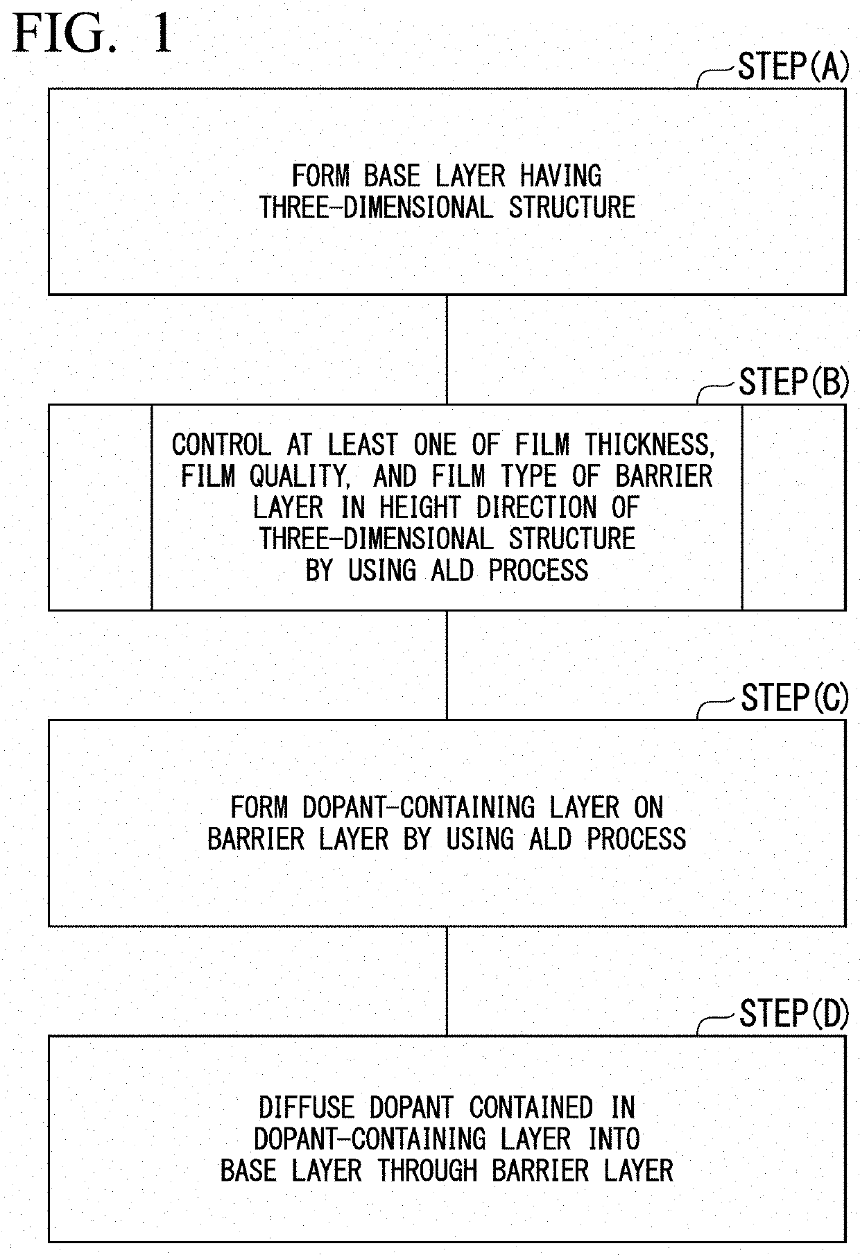
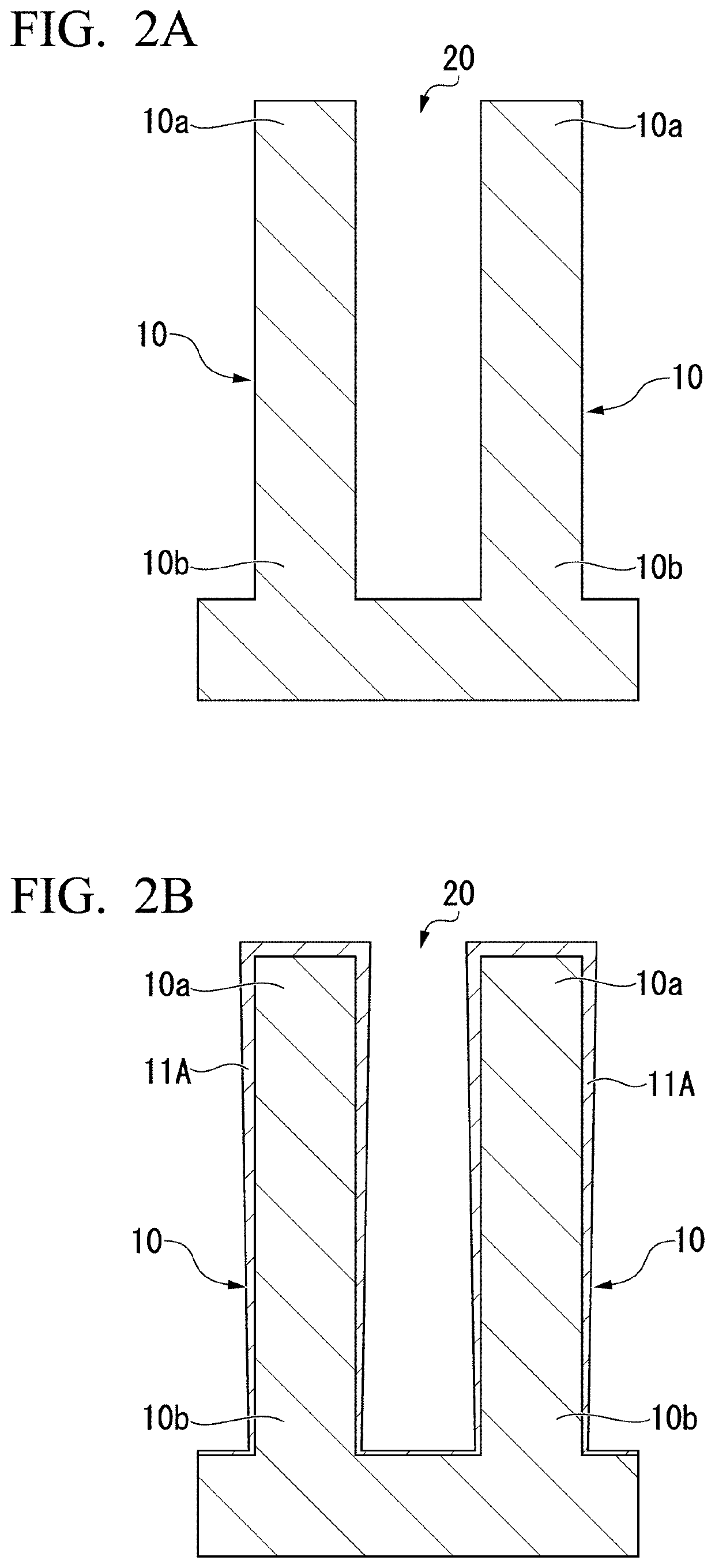
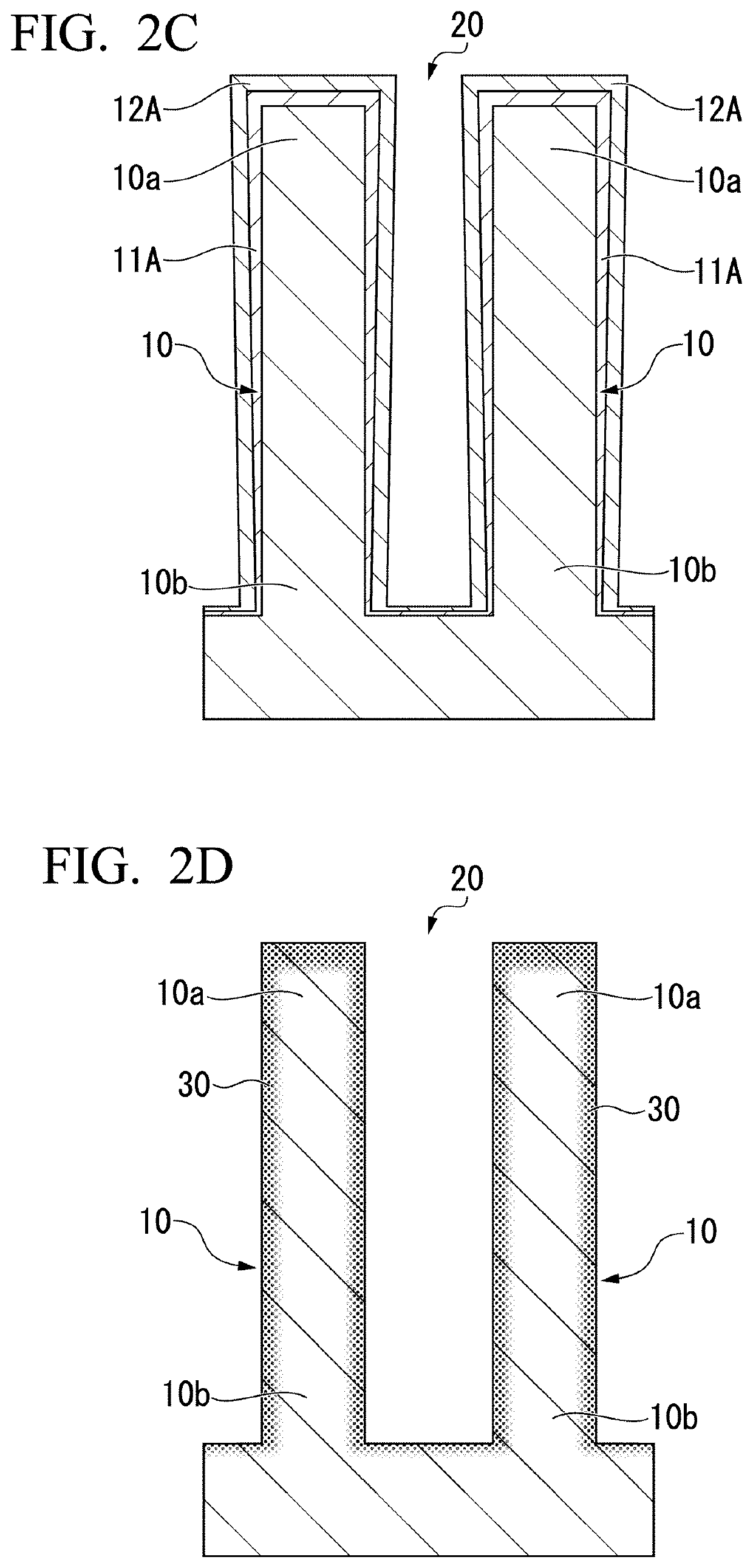
[0038]FIG. 1 is a flowchart illustrating a method for manufacturing a semiconductor device according to an embodiment of the present disclosure, and FIGS. 2A to 2D are schematic diagrams illustrating an example of steps (A) to (D) in FIG. 1, respectively.

[0039]As illustrated in FIG. 1, the method for manufacturing a semiconductor device according to an embodiment of the present disclosure includes a step (A) of forming a base layer having a three-dimensional structure, a step (B) of forming a barrier layer on the base layer, a step (C) of forming a dopant-containing layer on the barrier layer by...


PUM

PropertyMeasurementUnit
aspect ratioaaaaaaaaaa
thicknessaaaaaaaaaa
thicknessaaaaaaaaaa

Abstract

In a method for forming a barrier layer, the barrier layer is formed on a base layer having a three-dimensional structure before a dopant-containing layer is formed on the base layer. At this time, at least one of a film thickness, a film quality, and a film type of the barrier layer is controlled in a height direction of the three-dimensional structure by using an atomic layer deposition (ALD) process.

Description

CROSS-REFERENCE TO RELATED APPLICATIONS[0001]This application claims the benefit of and priority to U.S. Provisional Application No. 63 / 005,156, filed on Apr. 3, 2020 in the United States Patent and Trademark Office, the disclosure of which is incorporated herein in its entirety by reference.BACKGROUND OF THE INVENTIONField of the Invention[0002]The present disclosure relates to a method for forming a barrier layer and a method for manufacturing a semiconductor device, and more particularly, to a method for forming a barrier layer which is used for doping a base layer in a manufacturing process of a semiconductor device such as a FinFET.Description of Related Art[0003]Conventionally, with high integration of a semiconductor chip, miniaturization, a high-speed operation, and low power consumption of a planar transistor such as a MOSFET have been progressed. However, in a conventional planar transistor, a so-called short channel effect, which cannot control an operation by a gate volt...

Claims


Application Information

Patent Timeline
Patent Type & Authority Applications(United States)
IPC IPC(8): H01L21/225H01L21/02
CPCH01L21/2254H01L21/0217H01L29/66803H01L21/0228H01L21/02274H01L21/02164H01L29/66795H01L21/02211H01L21/02219H01L21/0214H01L21/02129H01L21/022H01L21/2256H01L21/2252H01L21/2225C23C16/045C23C16/345C23C16/308C23C16/45529C23C16/4554C23C16/52
Inventor NAKANO, RYU
Owner ASM IP HLDG BV
Why Eureka
Try Eureka