

Solid-state imaging device and imaging device
a solid-state imaging and imaging device technology, applied in semiconductor devices, radio frequency controlled devices, electrical devices, etc., can solve the problems of difficult acquisition and difficult to cope with a case where relatively high-speed processing is required, and achieve the effect of improving the light-reception efficiency
- Summary
- Abstract
- Description
- Claims
- Application Information
AI Technical Summary
Benefits of technology
Problems solved by technology
Method used
Image

Examples
first embodiment
2. First Embodiment
[0116]First, a solid-state imaging device and an imaging device according to a first embodiment will be described in detail with reference to the accompanying drawings.
[0117]2.1 Configuration Example of Imaging Device
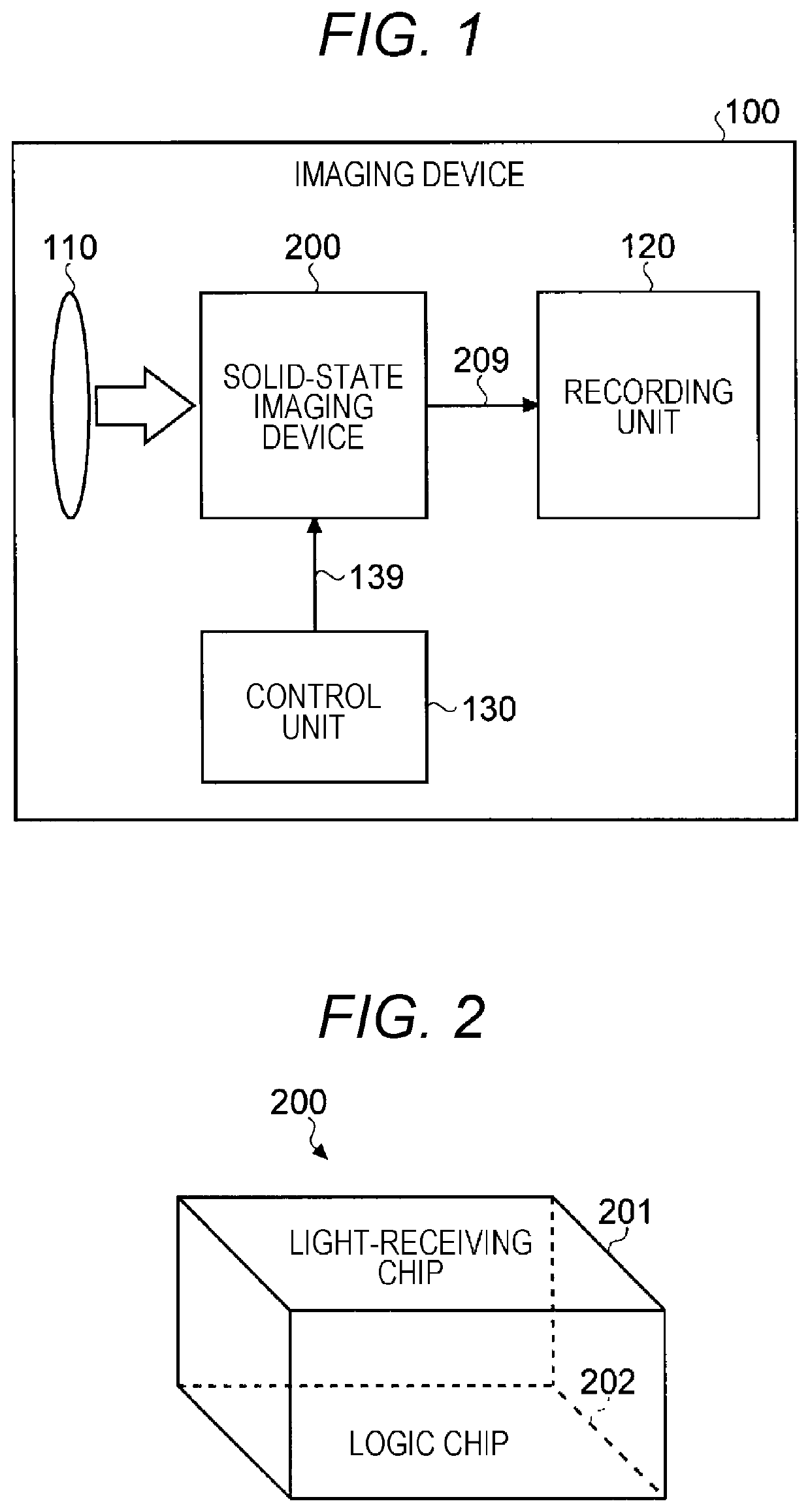
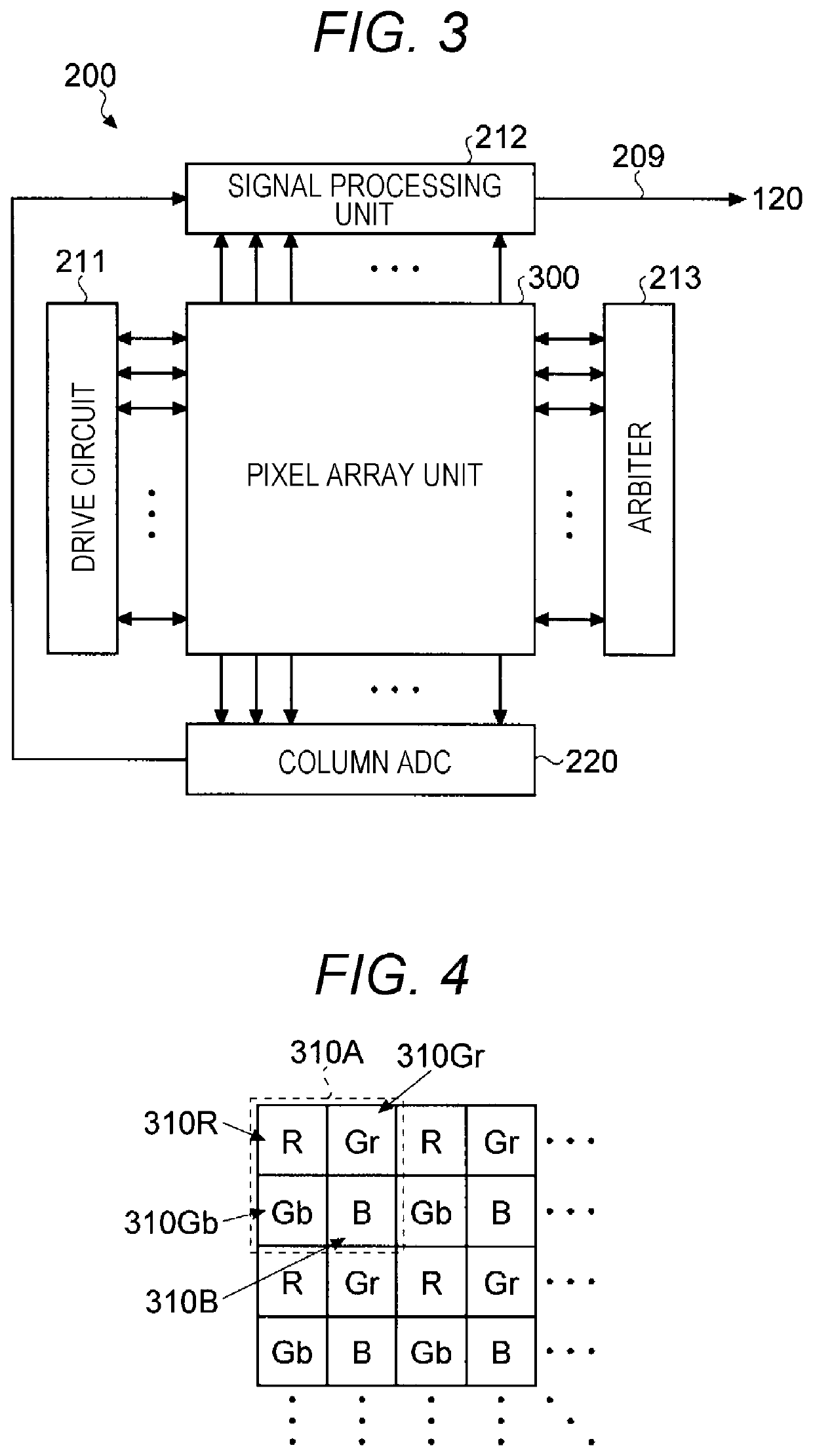
[0118]FIG. 1 is a block diagram illustrating a schematic configuration example of the solid-state imaging device and the imaging device according to the first embodiment. As illustrated in FIG. 1, for example, an imaging device 100 includes an imaging lens 110, a solid-state imaging device 200, a recording unit 120, and a control unit 130. As the imaging device 100, a camera that is mounted in an industrial robot, an in-vehicle camera, and the like are assumed.
[0119]The imaging lens 110 is an example of an optical system that condenses incident light and images an image of the incident light to a light-receiving surface of the solid-state imaging device 200. The light-receiving surface is a surface on which photoelectric conversion elements in the sol...
second embodiment
3. Second Embodiment
[0290]Next, a solid-state imaging device and an imaging device according to a second embodiment will be described in detail with reference to the accompanying drawing. Furthermore, in the following description, with regard to configurations similar to those in the above-described embodiment, the configurations will be cited, and redundant description thereof will be omitted.
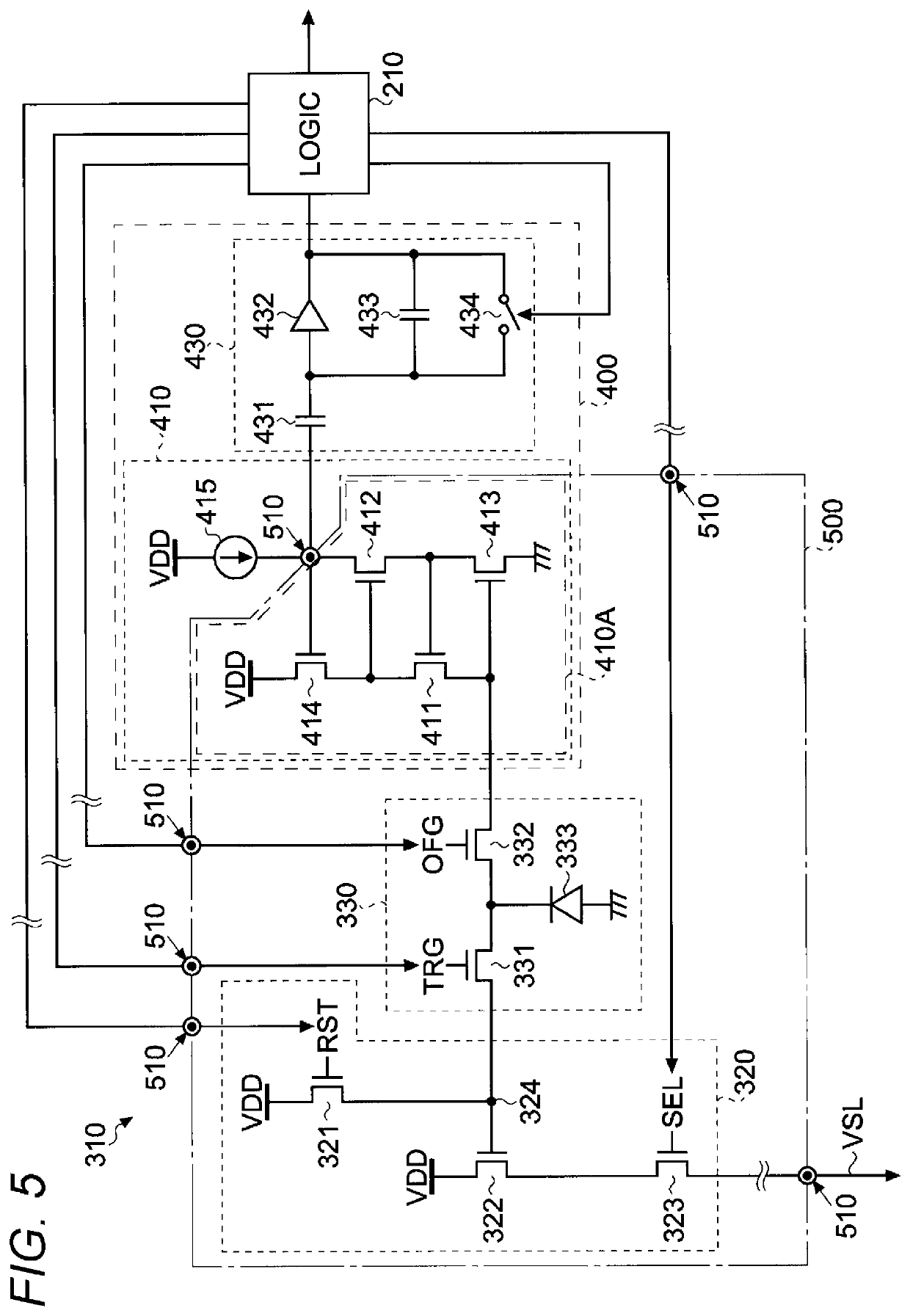
[0291]For example, it is necessary for the capacity of the photoelectric conversion element 333 to be small in order for the address event to be ignited with sensitivity with respect to incident light. On the other hand, it is necessary for the capacity of the photoelectric conversion element 333 to be large to widen a dynamic range of an image that is acquired. Therefore, in this embodiment, the capacity of the photoelectric conversion element 333 is switched between a period of monitoring the address event ignition and a period of reading out a pixel signal.
[0292]For example, the imaging dev...
third embodiment
4. Third Embodiment
[0344]Next, a solid-state imaging device and an imaging device according to a third embodiment will be described in detail with reference to the accompanying drawings. Furthermore, in the following description, with regard to configurations similar to those in the above-described embodiments, the configurations will be cited, and redundant description thereof will be omitted.
[0345]In the second embodiment, description has been given of a case where the photoelectric conversion element 333 is divided into two photoelectric conversion elements 3331 and 3332 by providing the photogate 601. In contrast, in the third embodiment, a photoelectric conversion element of which a capacity is substantially variable is used instead of the photoelectric conversion element 333 with a fixed capacity.
[0346]An imaging device and a solid-state imaging device according to this embodiment may be similar to, for example, the imaging device 100 and the solid-state imaging device 200 des...
PUM
| Property | Measurement | Unit |
|---|---|---|
| velocity | aaaaa | aaaaa |
| photoelectric | aaaaa | aaaaa |
| distance | aaaaa | aaaaa |
Abstract
Description
Claims
Application Information