Three-dimensional flash memory including middle metallization layer and manufacturing method thereof

Pending Publication Date: 2021-10-21
SAMSUNG ELECTRONICS CO LTD
View PDF0 Cites 1 Cited by
  • Summary
  • Abstract
  • Description
  • Claims
  • Application Information

AI Technical Summary

Benefits of technology

The patent proposes a method of manufacturing a three-dimensional flash memory that solves problems of degraded material and high cost in conventional manufacturing technology. It also proposes a three-dimensional flash memory that overcomes limitations of miniaturization and integration in the horizontal direction. The flash memory includes at least one intermediate wiring layer that increases cell current, reduces degradation in cell characteristic, supports bulk erase operation, enhances degree of integration, and simplifies wiring process. The patent also includes various shapes of the intermediate wiring layer, such as a plate shape or a line shape, which all provide the same benefits. Overall, the technical effects of this patent include improved manufacturing process and enhanced performance of the three-dimensional flash memory.

Problems solved by technology

However, conventional manufacturing technology including at least one intermediate wiring layer formed of tungsten (W) has a problem, in which a material of the at least one intermediate wiring layer is inevitably degraded in a process of forming a channel layer with poly-silicon (poly-Si) at a high temperature of 600° C. or more in a process of forming an upper string, and a drawback in that a W layer forming process is a process having a relatively high cost.

Method used


Image

  • Three-dimensional flash memory including middle metallization layer and manufacturing method thereof
  • Three-dimensional flash memory including middle metallization layer and manufacturing method thereof
  • Three-dimensional flash memory including middle metallization layer and manufacturing method thereof

Examples


first embodiment

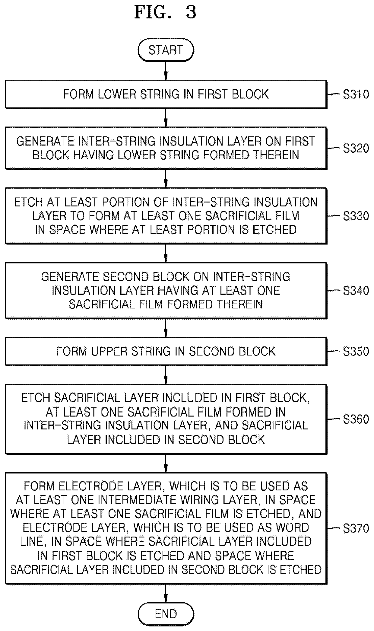
[0062]FIGS. 4A to 4J are diagrams illustrating a first embodiment for describing the method of manufacturing a three-dimensional flash memory illustrated in FIG. 3;

[0063]FIGS. 5A to 5C are diagrams illustrating three-dimensional flash memories having various structures manufactured by the method of manufacturing a three-dimensional flash memory illustrated in FIG. 3;

second embodiment

[0064]FIGS. 6A to 6G are diagrams illustrating a second embodiment for describing the method of manufacturing the three-dimensional flash memory illustrated in FIG. 3;

[0065]FIG. 7 is a diagram illustrating a three-dimensional flash memory having various structures manufactured by the method of manufacturing a three-dimensional flash memory illustrated in FIGS. 6A to 6G;

third embodiment

[0066]FIGS. 8A to 8G are diagrams illustrating a third embodiment for describing the method of manufacturing a three-dimensional flash memory illustrated in FIG. 3;

[0067]FIG. 9 is a diagram illustrating a three-dimensional flash memory having another structure manufactured by the method of manufacturing a three-dimensional flash memory illustrated in FIGS. 8A to 8G;

[0068]FIG. 10 is a flowchart illustrating a method of manufacturing a three-dimensional flash memory according to another embodiment;

[0069]FIGS. 11A to 11G are diagrams illustrating an embodiment for describing the method of manufacturing a three-dimensional flash memory illustrated in FIG. 10;

[0070]FIG. 12 is a top view of a three-dimensional flash memory for describing a structure of a bit line of the related art;

[0071]FIG. 13 is a top view illustrating a three-dimensional flash memory having a bit line structure according to an embodiment;

[0072]FIG. 14 is a cross-sectional view for describing an intermediate wiring lay...


PUM


Abstract

A three-dimensional flash memory including an intermediate wiring layer and a method of manufacturing the same are disclosed. According to an embodiment, a method of manufacturing a three-dimensional flash memory by using a back end process includes: forming a lower string in a first block, the first block including a sacrificial layer and an insulation layer which are formed to extend in a first direction and are alternately stacked; generating an inter-string insulation layer on the first block that has the lower string formed therein; etching at least a portion of the inter-string insulation layer to form at least one sacrificial film in a space where the at least a portion is etched; generating a second block on the inter-string insulation layer, where the at least one sacrificial film is formed, the second block including a sacrificial layer and an insulation layer which are formed to extend in the first direction and are alternately stacked; forming an upper string in the second block; etching the sacrificial layer included in the first block, the at least one sacrificial film, and the sacrificial layer included in the second block; and forming an electrode layer, which is to be used as at least one intermediate wiring layer, in a space where the at least one sacrificial film is etched, and an electrode layer, which is to be used as a word line, in a space where the sacrificial layer included in the first block is etched and a space where the sacrificial layer included in the second block is etched.

Description

TECHNICAL FIELD[0001]The following embodiments relate to a method of manufacturing a three-dimensional flash memory, and more particularly, to a three-dimensional flash memory including an intermediate wiring layer.BACKGROUND ART[0002]A flash memory device may be electrically erasable programmable read only memory (EEPROM) which is electrically erasable and programmable, and the memory may be commonly used for, for example, a computer, a digital camera, an MP3 player, a game system, a memory stick, etc. The flash memory device electrically controls input / output of data through Fowler-Nordheim (F-N) tunneling or hot electron injection.[0003]In detail, referring to FIG. 1 illustrating an array of a three-dimensional flash memory of the related art, the array of the three-dimensional flash memory may include a common source line CSL, a bit line BL, and a plurality of cell strings CSTR arranged between the common source line CSL and the bit line BL.[0004]Bit lines are two-dimensionally ...

Claims


Application Information

Patent Timeline
IPC IPC(8): G11C16/04H01L27/11519H01L27/11582H01L27/11521H01L27/11556H01L27/11565H01L27/11568H01L23/528
CPCG11C16/0483H01L27/11519H01L27/11582H01L23/5283H01L27/11556H01L27/11565H01L27/11568H01L27/11521G11C16/26H10B43/10H10B43/27H10B41/10H10B41/27H10B41/30H10B43/30
Inventor SONG, YUN HEUB
Owner SAMSUNG ELECTRONICS CO LTD
Why Eureka
Try Eureka