Thermochemical Gas Sensor Using Thermoelectric Thin Film And Method Of Manufacturing The Same
- Summary
- Abstract
- Description
- Claims
- Application Information
AI Technical Summary
Benefits of technology
Problems solved by technology
Method used
Image
Examples
example 1
[0129]A substrate, on which an insulating layer was formed, was used as a matrix of a device, and a seed layer was formed on the insulating layer. Subsequently, a thermoelectric material was plated on the seed layer using a wet electrolytic deposition method to form a thermoelectric thin film. Subsequently, an electrode was formed on the thermoelectric thin film, and a catalyst layer was formed on the electrode. As a result, a novel thermoelectric thin film-based thermochemical gas sensor was manufactured.
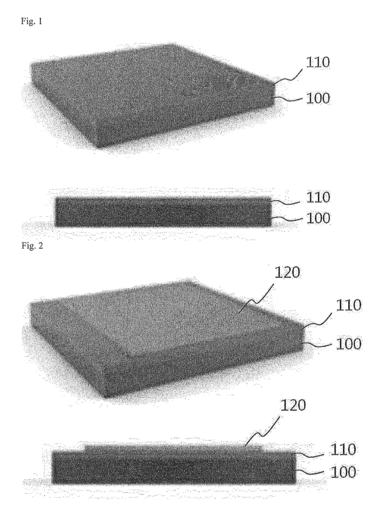
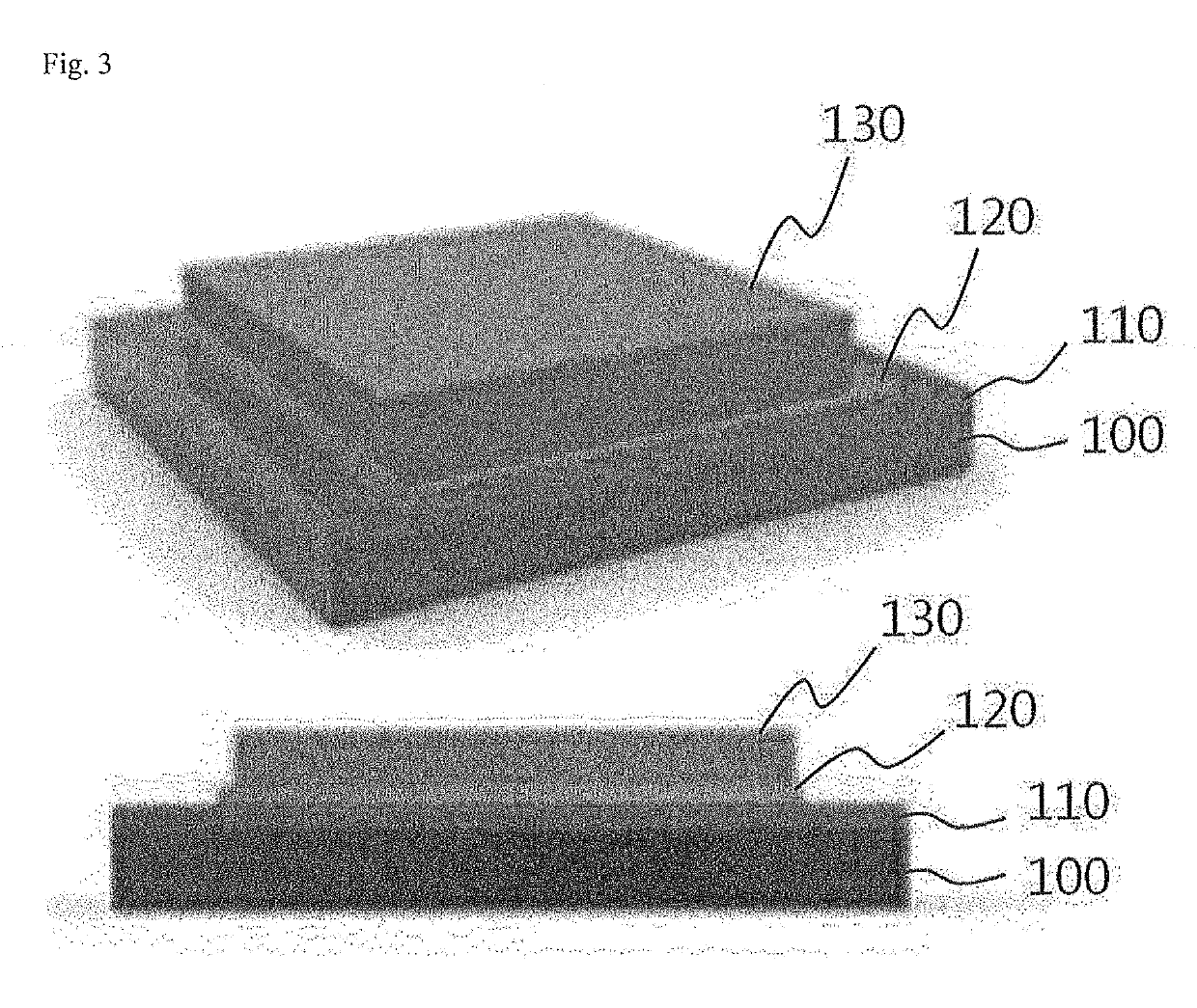
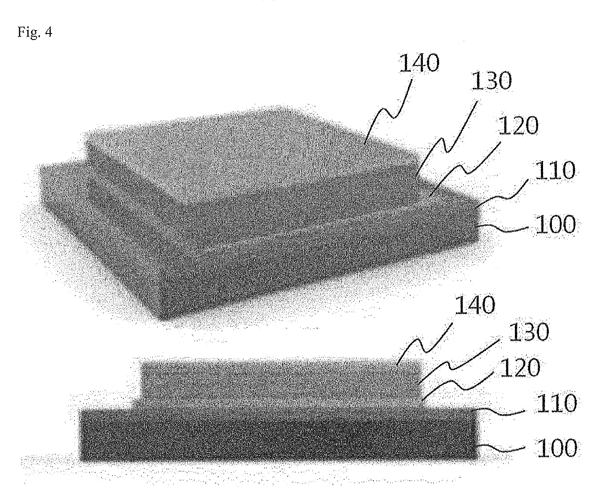
[0130]FIGS. 1 to 6 illustrate a method of manufacturing a thermochemical gas sensor according to Example 1.
[0131]Referring to FIGS. 1 to 6, a substrate 100 provided with an insulating layer 110 was prepared to manufacture the thermochemical gas sensor. The substrate 100 may include a silicon (Si) substrate. The insulating layer 110 may include a SiO2 oxide film.
[0132]A seed layer 120 was formed on the insulating layer 110. The seed layer 120 preferably has a thickness of 10 to 1000...
example 2
[0157]A substrate, on which an insulating layer was formed, was used as a matrix of a device, and seed layers were formed on the insulating layer. Subsequently, a thermoelectric material was plated on the seed layers using a wet electrolytic deposition method to form P-type and N-type thermoelectric thin films. Subsequently, electrodes were formed on the P-type and N-type thermoelectric thin films to maximize thermoelectric properties of a device through an N-P junction, and a catalyst layer was formed on the electrodes. As a result, a novel thermoelectric thin film-based thermochemical gas sensor was manufactured.
[0158]FIGS. 7 to 14 illustrate a method of manufacturing a thermochemical gas sensor according to Example 2.
[0159]Referring to FIGS. 7 to 14, a substrate 100 provided with an insulating layer 110 was prepared to manufacture the thermochemical gas sensor. The substrate 100 may include a silicon (Si) substrate. The insulating layer 110 may include a SiO2 oxide film.
[0160]See...
experimental example 1
[0183]A silicon wafer having a thickness of 500 μm, a width of 2.5 cm, and a length of 2.5 cm was used as a substrate. An oxide layer was formed on the silicon wafer.
[0184]To manufacture a single-type thermoelectric device on the silicon wafer, a gold seed layer was formed on the silicon wafer, on which an oxide layer has been formed, through an electron beam (E-beam). The thickness (height) of the formed seed layer was about 200 nm.
[0185]To find optimal conditions for thermoelectric thin film formation, a reduction potential under each condition was measured using cyclic voltammetry. The seed layer was electroplated while applying a voltage of 50 mV for one hour using a three-electrode system by means of a constant rectifier. Electrolytes used for the electroplating were prepared by adding 0 mM, 10 mM, and 40 mM of Bi(NO3)3.5H2O to a solution composed of 1 M of HNO3, 0.5 M of C4H6O6, and 10 mM of TeO2 to vary the concentration of Bi3+.
[0186]FIG. 15 illustrates results of Bi3+ conce...
PUM
| Property | Measurement | Unit |
|---|---|---|
| Thickness | aaaaa | aaaaa |
| Length | aaaaa | aaaaa |
| Concentration | aaaaa | aaaaa |
Abstract
Description
Claims
Application Information


