Organic light emitting diode dual screen display

a light-emitting diode and organic technology, applied in the field of display technologies, can solve the problems of increased production cost, thicker display, complex structure and process, etc., and achieve the effect of further reducing production cos

Active Publication Date: 2021-10-28
SHENZHEN CHINA STAR OPTOELECTRONICS SEMICON DISPLAY TECH CO LTD
View PDF0 Cites 0 Cited by
  • Summary
  • Abstract
  • Description
  • Claims
  • Application Information

AI Technical Summary

Benefits of technology

[0017]In comparison with the prior art, in the OLED dual screen display provided in the embodiments of the present disclosure, the two edges of the two OLED display panels are adhe...

Problems solved by technology

The existing OLED dual screen display combines two independent OLED backplanes back-to-back to achieve dual screen display, resulting in a thicker dis...

Method used


Image

  • Organic light emitting diode dual screen display
  • Organic light emitting diode dual screen display

Examples


first embodiment

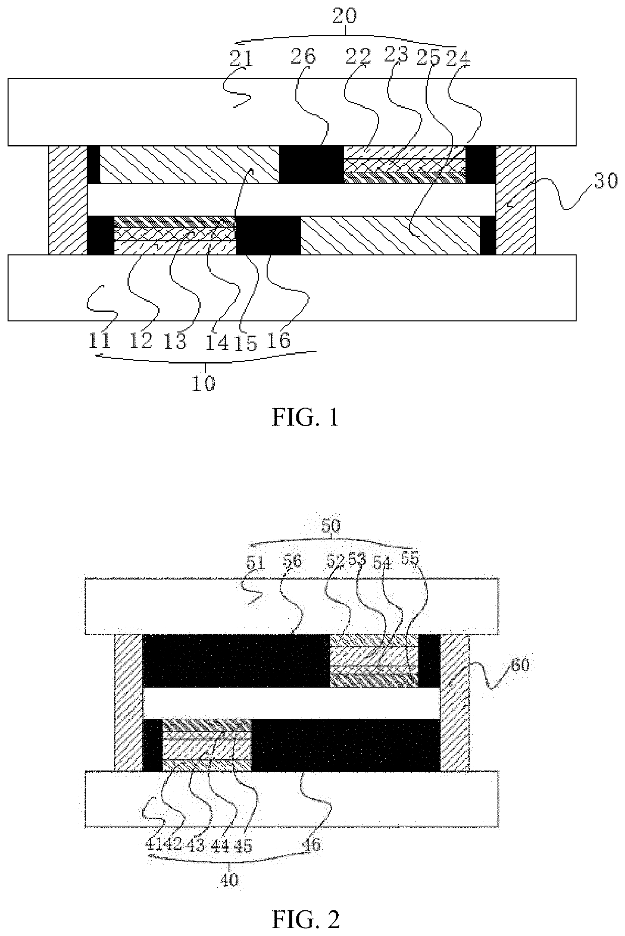
[0033]In the OLED dual screen display of the present disclosure, the first TFT array layer 12, the first OLED organic light emitting layer 13, the first reflective cathode layer 14, and the first color filter layer 15 of the first OLED display panel 10 constitute a sub-pixel. The second TFT array layer 22, the second OLED organic light emitting layer 23, the second reflective cathode layer 24, and the second color filter layer 25 of the second OLED display panel 20 constitute another sub-pixel. Therefore, the OLED dual screen display achieves a double-sided display.

[0034]A light emitting direction of the first OLED display panel 10 is close to one side of the second OLED display panel 20, that is, it faces the second substrate 21. Specifically, the light emitted by the first OLED organic light emitting layer 13 is reflected by a reflective anode of the first substrate 11 and passes through the semi-transparent first cathode layer 14 to the first color filter layer 15 and is finally ...

second embodiment

[0036]As shown in FIG. 2, an embodiment of the present disclosure also provides another structure of an OLED dual screen display. the OLED dual screen display is a bottom-emitting structure. A first OLED display panel 40 and a second OLED display panel 50 are both non-color filter on array (COA) substrates.

[0037]Specifically, the OLED dual screen display includes the first OLED display panel 40 and the second OLED display panel 50 opposite to the first OLED display panel 40. Both edges of the first OLED display panel 40 and both edges of the second OLED display panel 50 are adhered by a sealant 60. Both the first OLED display panel 40 and the second OLED display panel 50 include an open area and a non-open area, and the non-open area is provided with a black matrix.

[0038]Specifically, the first OLED display panel 40 includes a first substrate 41, a first color filter layer 42, a first thin film transistor (TFT) array layer 43, a first OLED organic light emitting layer 44, a first re...


PUM


Abstract

An organic light emitting diode (OLED) dual screen display is provided, including a first OLED display panel and a second OLED display panel opposite to the first OLED display panel. Both edges of the first OLED display panel and both edges of the second OLED display panel are adhered by a sealant. Both the first OLED display panel and the second OLED display panel include an open area and a non-open area, and the non-open area is provided with a black matrix.

Description

FIELD OF DISCLOSURE[0001]The present disclosure relates to the field of display technologies, and in particular, to an organic light emitting diode (OLED) dual screen display.BACKGROUND[0002]Dual screen displays have broad application prospects in the fields of commodity displays, electronic bulletin boards, and high-end exhibitions. Conventional liquid crystal displays (LCDs) dual screen technology is implemented by two LCD display panels laminated back to back. Both display panels need respective backlights, and there is a need for a design of heat dissipation, so that the manufactured dual screen display will have a large thickness and occupy space to affect a look-and-feel, and the process is complicated and a yield is low, so a production cost is high.[0003]In comparison to LCDs, organic light emitting diode (OLED) displays do not require a separate backlight and have self-luminous characteristics. With very thin coatings of organic materials and glass substrates, these organic...

Claims


Application Information

Patent Timeline
IPC IPC(8): H01L27/32H01L25/065H01L51/52
CPCH01L27/3267H01L25/0657H01L51/0096H01L27/3276H01L51/5284G09F9/33H10K59/12H10K50/8426H10K19/901H10K59/38H10K59/128H10K59/176H10K59/131H10K50/865H10K77/10
Inventor HOU, JIDA
Owner SHENZHEN CHINA STAR OPTOELECTRONICS SEMICON DISPLAY TECH CO LTD
Why Eureka
Try Eureka