
OLED display panel, manufacturing method thereof, and OLED display device

a technology of light-emitting diodes and display panels, which is applied in the direction of basic electric elements, semiconductor devices, electrical equipment, etc., can solve the problems of uneven film thickness, affecting the uniform illumination of pixel surfaces, and compromising light-emitting effects, so as to reduce the area improve device quality, and reduce the effect of pixel light-emitting regions

Active Publication Date: 2021-10-28
SHENZHEN CHINA STAR OPTOELECTRONICS SEMICON DISPLAY TECH CO LTD
View PDF0 Cites 0 Cited by
  • Summary
  • Abstract
  • Description
  • Claims
  • Application Information

AI Technical Summary

Benefits of technology

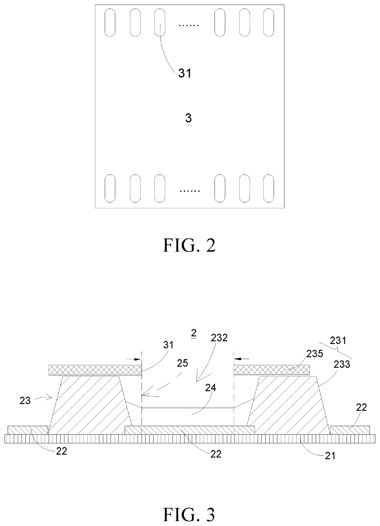
The present invention provides an OLED display panel and a manufacturing method with improved lighting uniformity and device quality. A light shielding layer is used to shield non-uniform illumination and color shift caused by unevenness of film formation at the edge light-emitting region, achieving concave / convex surface of a pixel light-emitting region. An optical film layer is also placed at a light shielding opening to further improve color uniformity and angles of view.

Problems solved by technology

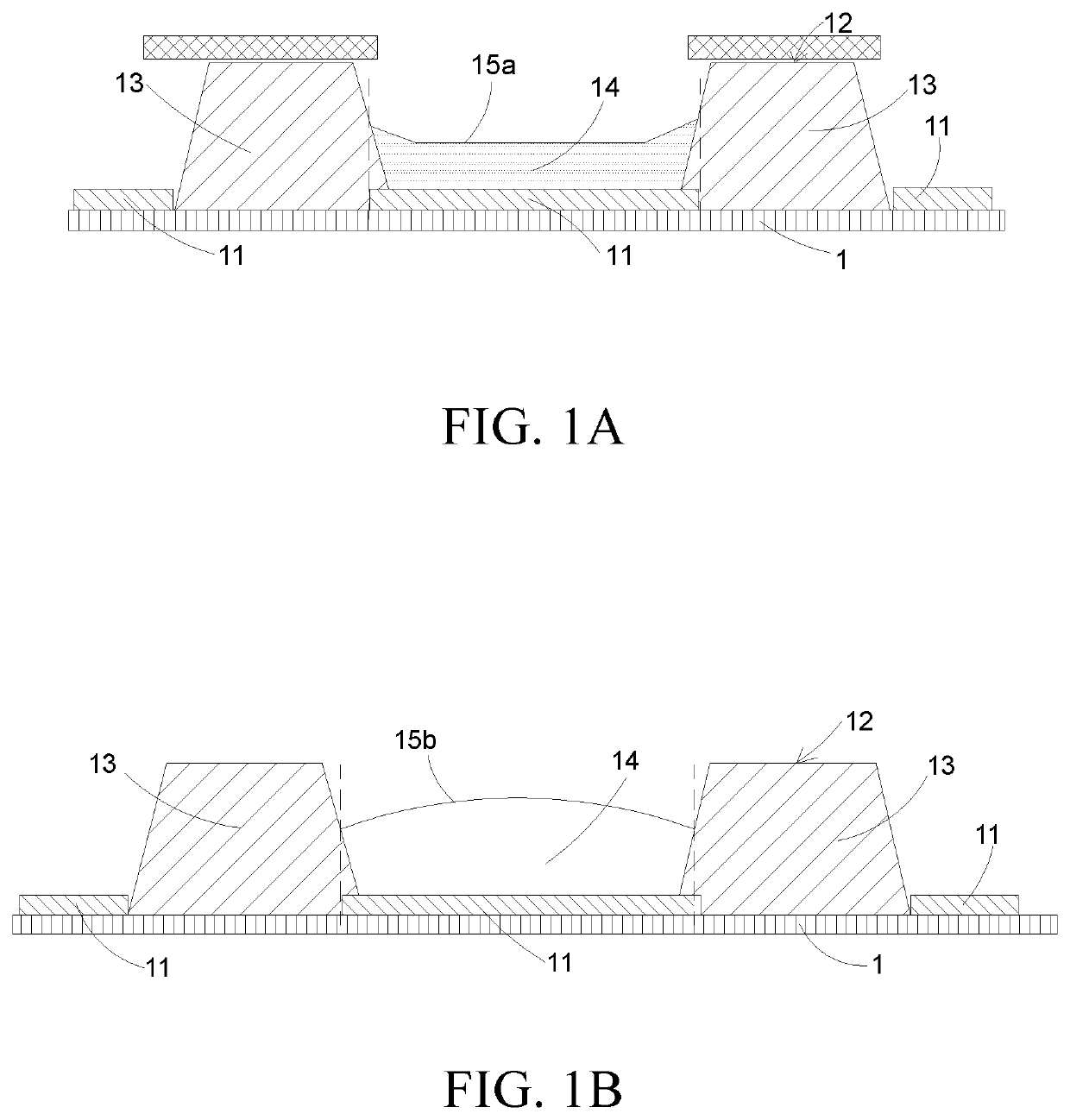
Due to ink infiltration or a coffee-ring effect at an edge of the bank 13, film formation quality after the ink 14 is dried is lowered, leading to uneven film thickness and uneven illumination in a light-emitting region, thus compromising a light-emitting effect.
In other words, this problem greatly affects pixel illumination uniformity of the conventional printed substrate 1.
Therefore, a convex or concave in-pixel film surface will cause uneven illumination, thereby affecting illumination uniformity in the pixels.

Method used


Image

  • OLED display panel, manufacturing method thereof, and OLED display device
  • OLED display panel, manufacturing method thereof, and OLED display device
  • OLED display panel, manufacturing method thereof, and OLED display device

Examples


Embodiment Construction

[0032]“Embodiment” in the following description means that specific features, structures or characteristics described in connection with the embodiment may be included in at least one embodiment of the present invention. The same terms appearing in different places in the specification are not necessarily limited to the same embodiment, but should be understood as an independent or alternative embodiment to other embodiments. Based on the technical solutions disclosed in the embodiments of the present invention, those skilled in the art can understand other combinations or modifications in accordance with the embodiments of the present invention.

[0033]Please refer to FIGS. 2 and 3. FIG. 2 is a planar view illustrating a light shielding layer of an organic light-emitting diode (OLED) display panel. FIG. 3 is a cross-sectional view illustrating the OLED display panel according to the present invention. As shown in the drawings, the present invention provides an OLED display panel 2. T...


PUM

PropertyMeasurementUnit
sizeaaaaaaaaaa
sizeaaaaaaaaaa
refractive indexaaaaaaaaaa

Abstract

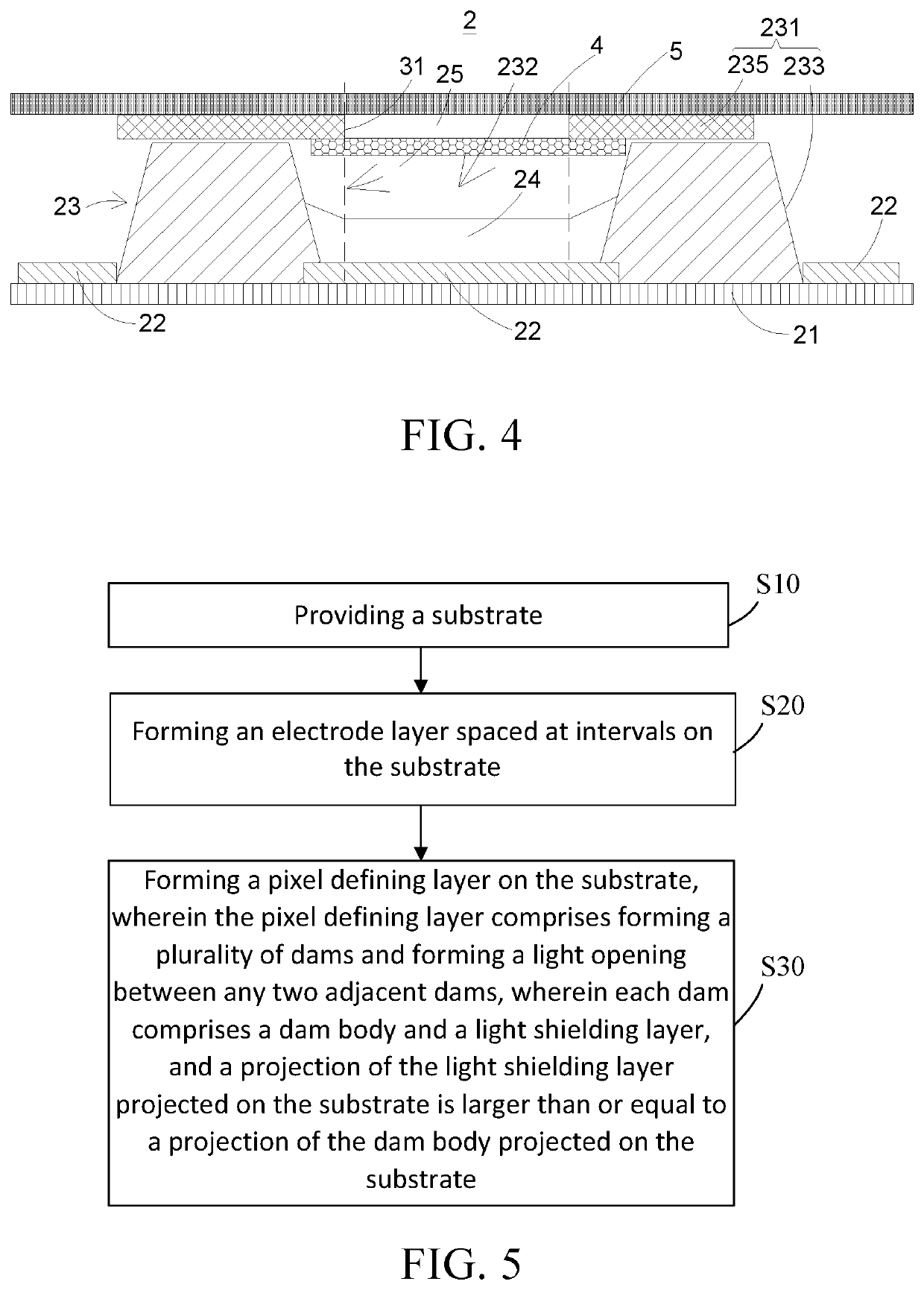
The present invention provides an organic light-emitting diode (OLED) display panel, a manufacturing method thereof, and a display device. The OLED display panel includes a substrate, an electrode layer, a pixel defining layer, and a light shielding layer. The electrode layer is spaced at intervals on the substrate. The pixel defining layer is placed on the substrate. The pixel defining layer includes dams and a light opening between any two adjacent dams. Each dam includes a dam body and a light shielding layer. A projection of the light shielding layer projected on the substrate is larger than or equal to a projection of the dam body projected on the substrate.

Description

1. FIELD OF DISCLOSURE[0001]The present invention relates to organic light-emitting diode (OLED) displays and in particular, to an OLED display panel, a manufacturing method thereof, and an OLED display device.2. DESCRIPTION OF RELATED ART[0002]An organic functional film layer of an organic light-emitting diode (OLED) device is manufactured by a vacuum thermal deposition method and a solution-casting method. The solution-casting method is further categorized into spin coating, ink-jet printing, screen printing, and etc. The solution-casting method is to apply a solution on a substrate first, and then remove a solvent in the solution by vacuum drying and heat drying by a hot furnace or a hot plate, so that a solid matter in the solution is precipitated on the substrate to form a film.[0003]To be specific, as shown in FIG. 1A and FIG. 1B, a pixel defining layer (PDL) 12 and a bank 13 of a printed substrate 1 are made by inkjet printing with ink 14. Due to ink infiltration or a coffee-...

Claims


Application Information

Patent Timeline
Patent Type & Authority Applications(United States)
IPC IPC(8): H01L27/32H01L51/52H01L51/56
CPCH01L27/3272H01L27/3246H01L2227/323H01L51/5275H01L51/56H01L51/5268H10K59/122H10K59/1201H10K59/877H10K59/879H10K71/00H10K59/8792H10K71/20H10K59/126H10K50/854H10K50/858
Inventor LI, XIANGLONG
Owner SHENZHEN CHINA STAR OPTOELECTRONICS SEMICON DISPLAY TECH CO LTD
Learn More