Spin element and magnetic memory
- Summary
- Abstract
- Description
- Claims
- Application Information
AI Technical Summary
Benefits of technology
Problems solved by technology
Method used
Image
Examples
first embodiment
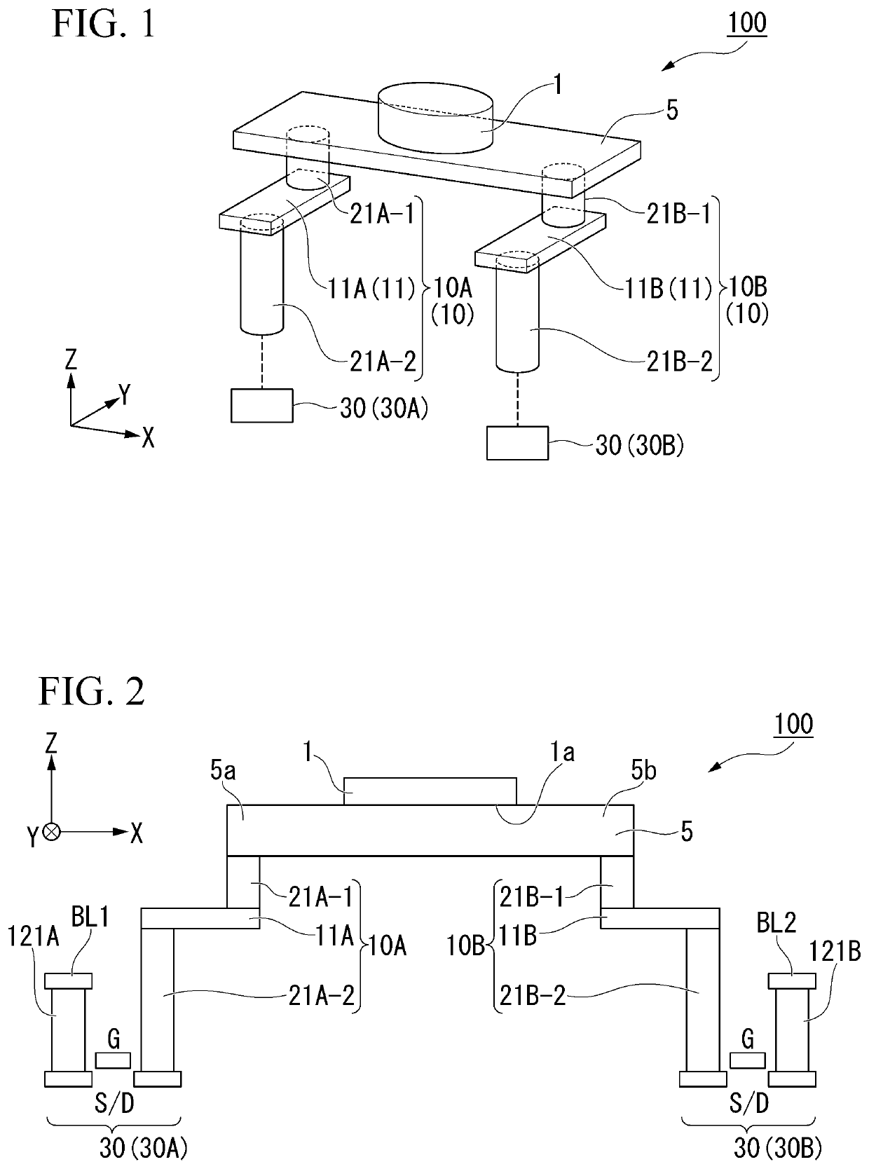
[0034]FIG. 1 is a perspective view schematically showing an SOT type magnetization rotational element 100 according to a first embodiment of the present invention. The SOT type magnetization rotational element is an example of the spin element.
[0035]The SOT type magnetization rotational element 100 has a first ferromagnetic layer 1, an SOT wiring 5, and a current path 10 (10A, 10B). The SOT wiring 5 is an example of the conducting portion. The first ferromagnetic layer 1 is an example of the element portion. In FIG. 1, a semiconductor circuit 30 connected to the SOT type magnetization rotational element 100 is also shown. The SOT wiring 5 extends in a first direction (X direction) as viewed in the direction of lamination of the first ferromagnetic layer 1 (Z direction). That is, the SOT wiring 5 has a long axis in the X direction in a plan view in the Z direction. The SOT wiring 5 faces the first ferromagnetic layer 1. Here, facing refers to a facing relationship in which the two la...
second embodiment
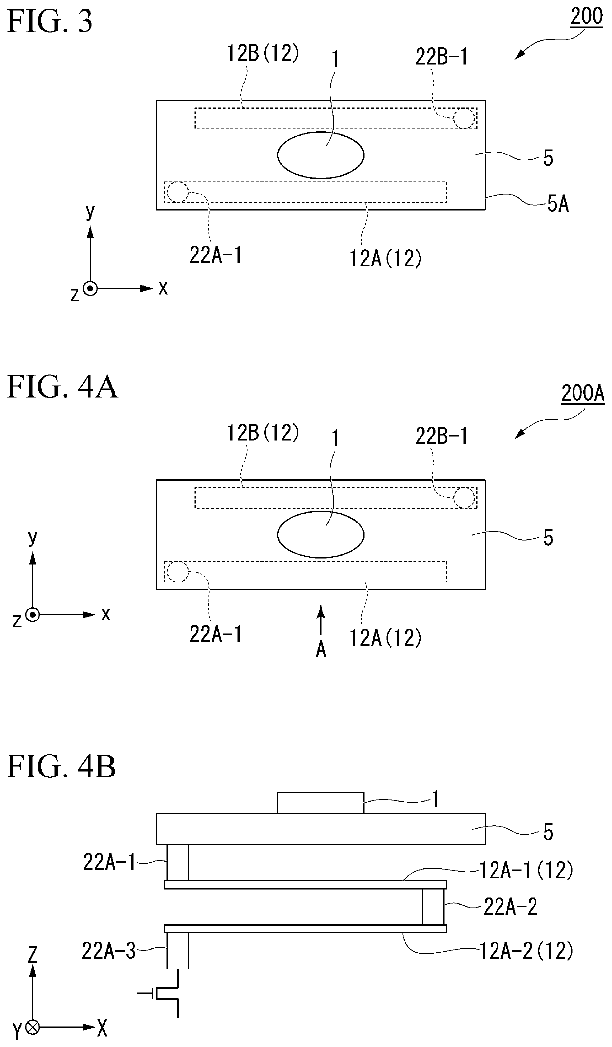
[0077]FIG. 3 is a schematic plan view of an SOT type magnetization rotational element 200 according to a second embodiment of the present invention as viewed in the Z direction.
[0078]Hereinafter, features of the SOT type magnetization rotational element 200 according to the second embodiment will be described. The same reference signs are assigned to components common with the SOT type magnetization rotational element 100 according to the first embodiment and a description thereof will be omitted.
[0079]In the SOT type magnetization rotational element 200, a resistance adjusting portion 12 is formed of two resistance adjusting parts 12A and 12B that are disposed apart from each other. The resistance adjusting portion 12 is within the range of an outer shape 5A of an SOT wiring 5 in a plan view in the Z direction. The two resistance adjusting parts 12A and 12B extend in the same X direction as the direction in which the SOT wiring 5 extends.
[0080]When the resistance adjusting portion ...
third embodiment
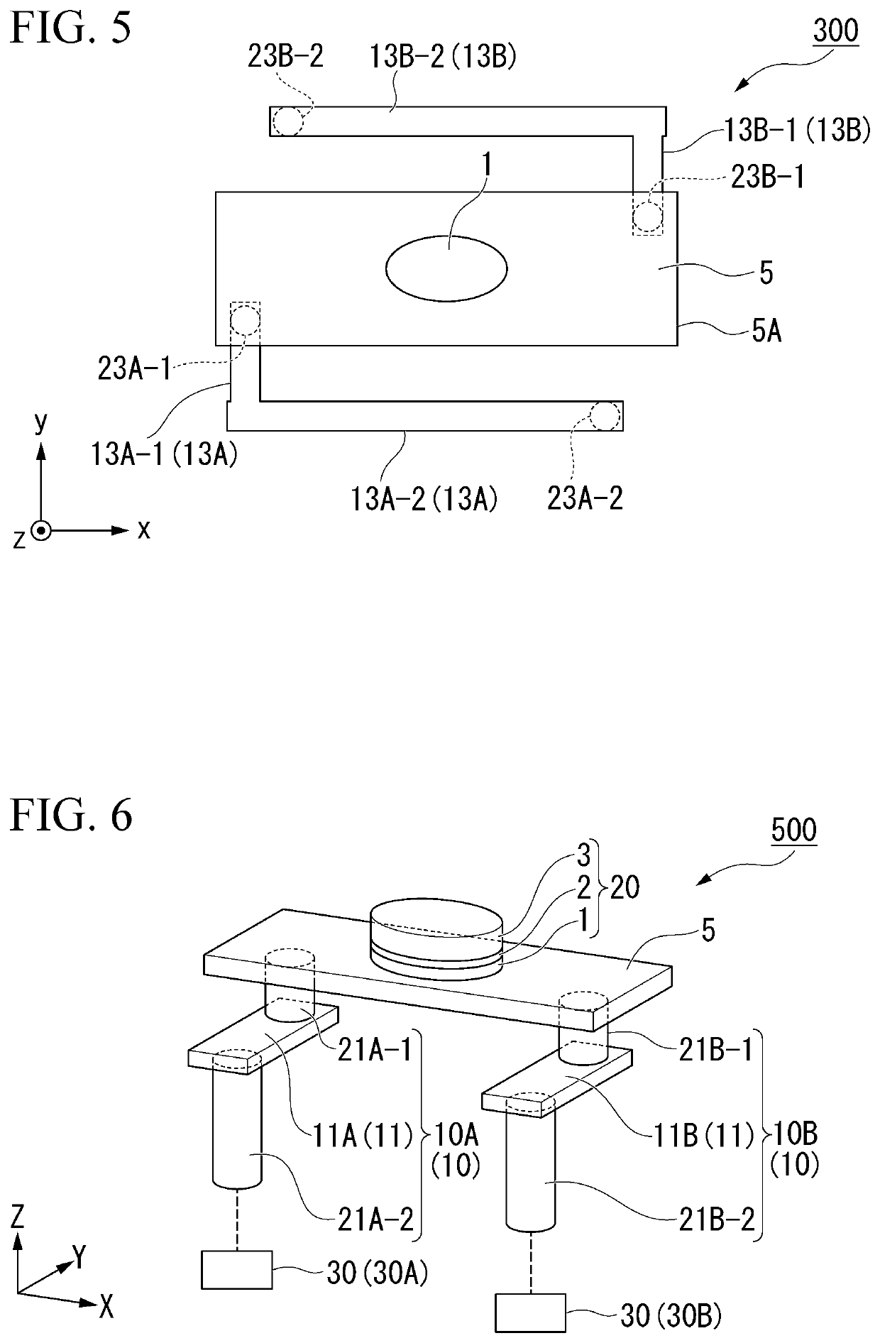
[0089]FIG. 5 is a schematic plan view of an SOT type magnetization rotational element 300 according to a third embodiment as viewed in the Z direction.
[0090]Hereinafter, features of the SOT type magnetization rotational element 300 according to the third embodiment will be described. The same reference signs are assigned to components common with the SOT type magnetization rotational element 100 according to the first embodiment and the SOT type magnetization rotational elements 200 and 200A according to the second embodiment and a description thereof will be omitted.
[0091]In the SOT type magnetization rotational element 300, a resistance adjusting portion 13 includes two resistance adjusting parts 13A and 13B that are disposed apart from each other. At least a part of the resistance adjusting parts 13A and 13B is disposed outside the range of an outer shape 5A of an SOT wiring 5 in a plan view in the lamination direction (Z direction). The two resistance adjusting parts 13A and 13B...
PUM
 Abstract
Description
Claims
Application Information
 - R&D
- Intellectual Property
- Life Sciences
- Materials
- Tech Scout
- Unparalleled Data Quality
- Higher Quality Content
- 60% Fewer Hallucinations
Browse by: Latest US Patents, China's latest patents, Technical Efficacy Thesaurus, Application Domain, Technology Topic, Popular Technical Reports.
© 2025 PatSnap. All rights reserved.Legal|Privacy policy|Modern Slavery Act Transparency Statement|Sitemap|About US| Contact US: help@patsnap.com


