
Eureka
For R&D, Eureka makes reading and utilizing patents & technical documents easy.
Eureka AIR
Designed for self-driven R&D workflows. Generate viable solutions, solve complex R&D challenges, empower your innovation with AI.

Eureka Materials
Designed for material experts only. Revolutionize your material R&D, from search, analyze, to developing new materials.

TechResearch
Generate reliable direction feasibility study reports for your R&D in just a few steps.

TechSeek
Discover and master advanced knowledge NOW. Basics, ideas, possibilities, all at once.

TechMind
As an expert in R&D Theories, TechMind can generates customized viable solutions instantly.

TechRisk
Analyze your overall solution with one click, know your potential R&D risks in advance.

TechMonitor
Get weekly tech updates, stay abreast of the latest tech innovations and key insights.
Solid-state imaging device and imaging device
- Summary
- Abstract
- Description
- Claims
- Application Information
AI Technical Summary
Benefits of technology
Problems solved by technology
Method used
Image

Examples
first embodiment
2. First Embodiment
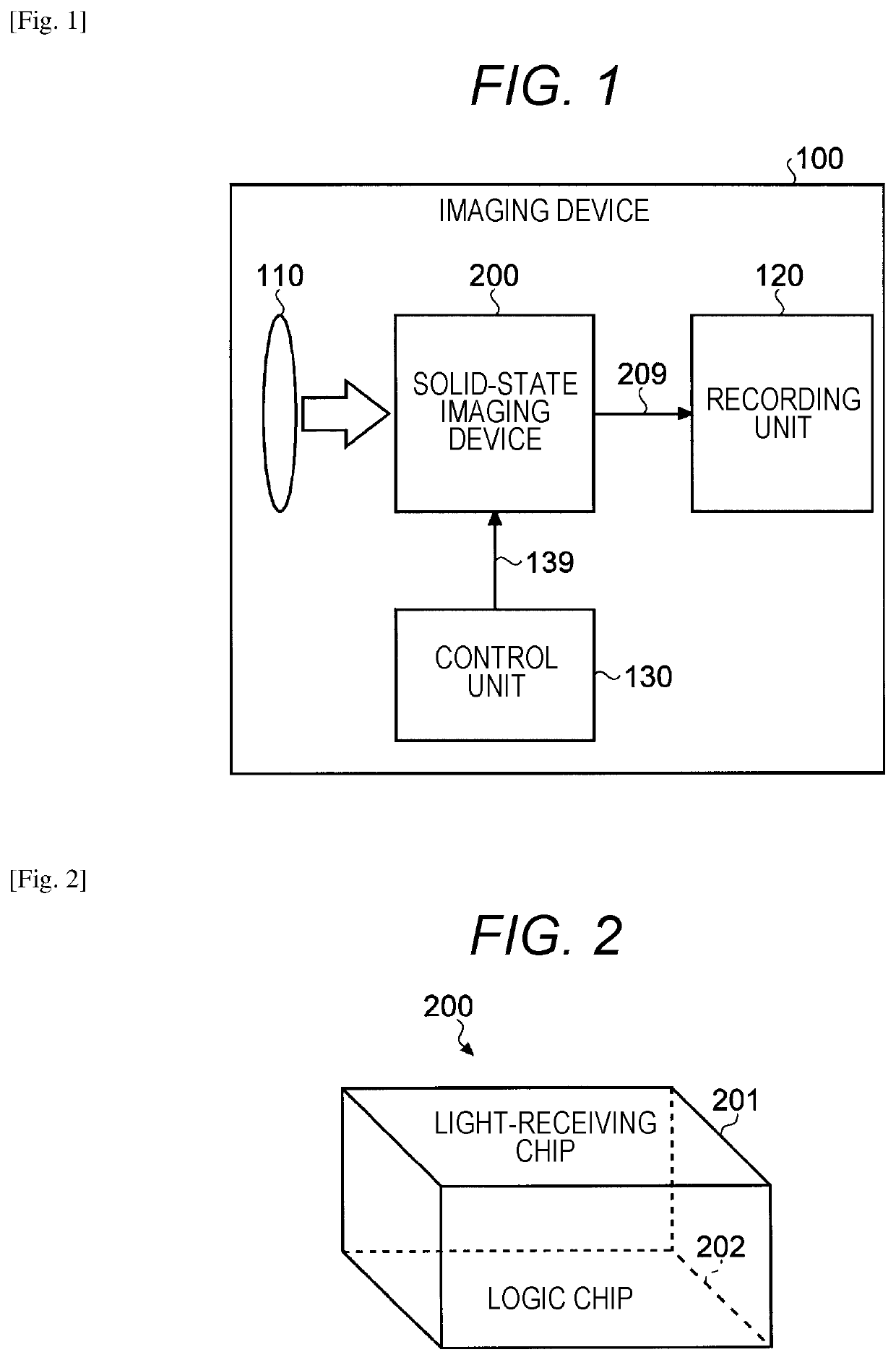
[0088]First, a solid-state imaging device and an imaging device according to a first embodiment of the present disclosure will be described in detail with reference to the accompanying drawings.
[0089]2.1 Configuration Example of Imaging Device
[0090]FIG. 1 is a block diagram illustrating a schematic configuration example of the solid-state imaging device and the imaging device according to the first embodiment. As illustrated in FIG. 1, for example, an imaging device 100 includes an imaging lens 110, a solid-state imaging device 200, a recording unit 120, and a control unit 130. As the imaging device 100, a camera that is mounted in an industrial robot, an in-vehicle camera, and the like are assumed.
[0091]The imaging lens 110 condenses incident light and images an image of the incident light to a light-receiving surface of the solid-state imaging device 200. The light-receiving surface is a surface on which photoelectric conversion elements (also referred to as “li...
second embodiment
3. Second Embodiment
[0233]Next, a solid-state imaging device and an imaging device according to a second embodiment will be described in detail with reference to the accompanying drawing. Furthermore, in the following description, with regard to configurations similar to those in the above-described embodiment, the configurations will be cited, and redundant description thereof will be omitted.
[0234]For example, as a method of improving sensitivity with respect to a charge that is generated in the photoelectric conversion element 333 in each of monitoring of address event ignition and reading-out of the pixel signal, a reduction in parasitic capacitance of the node 334 (for example, refer to FIG. 9) in the pixel block 310 is considered. Therefore, in this embodiment, for example, in a period of monitoring the address event ignition, the pixel signal generation unit 320 is separated from the node 334. With this arrangement, in a period of monitoring the address event ignition, it is ...
third embodiment
4. Third Embodiment
[0253]Next, a solid-state imaging device and an imaging device according to a third embodiment will be described in detail with reference to the accompanying drawings. Furthermore, in the following description, with regard to configurations similar to those in the above-described embodiments, the configurations will be cited, and redundant description thereof will be omitted.
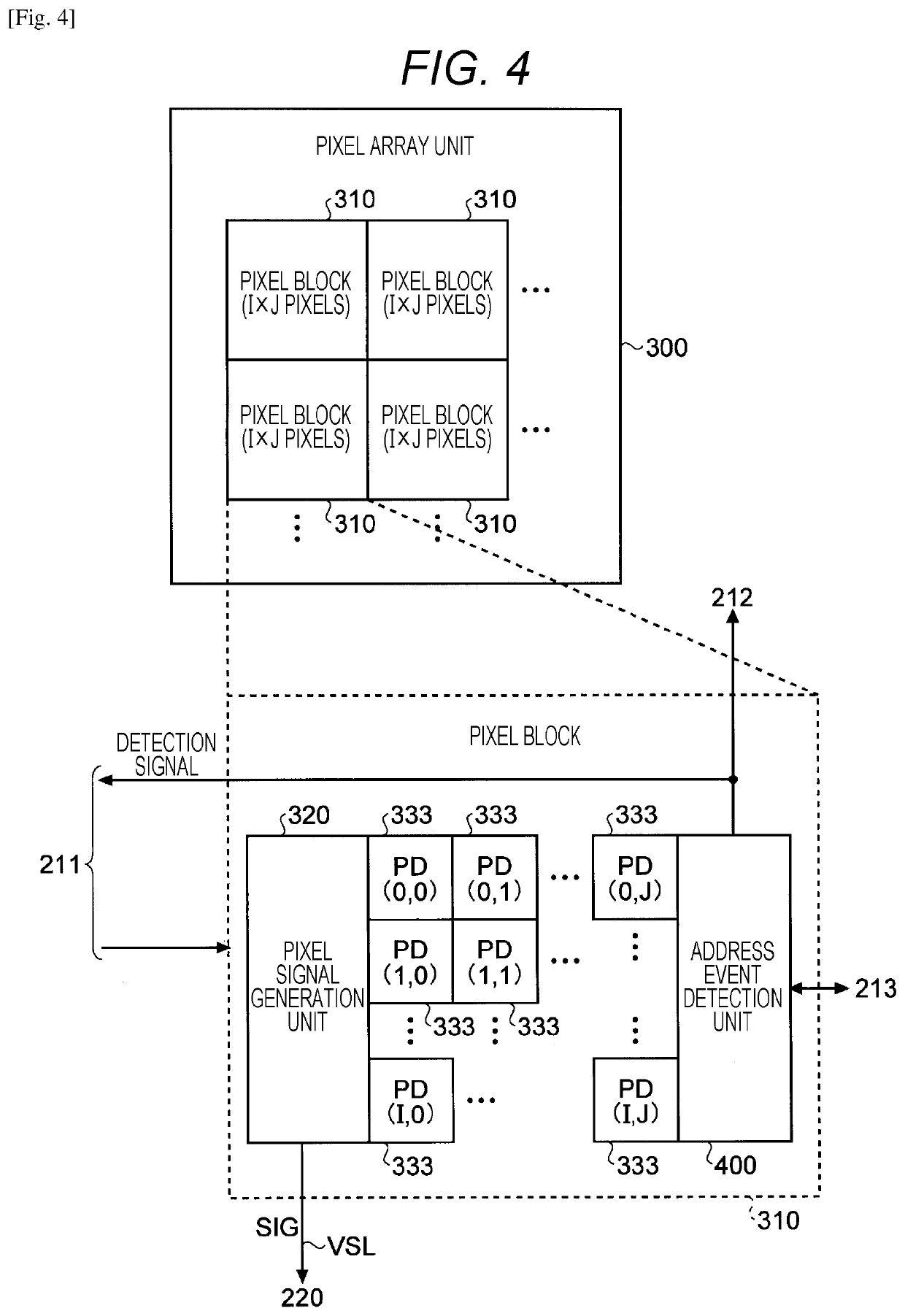
[0254]In the above-described embodiments, it is assumed that the number of the photoelectric conversion elements 333 in I rows×J columns which are included in the pixel block 310 or 610 is set to a total of four of 2×2 pixels. In other words, in the above-described embodiments, the pixel signal generation unit 320 and the address event detection unit 400 are shared by four pieces of the photoelectric conversion elements 333. In contrast, in the third embodiment, description will be given of a case where the number of the photoelectric conversion elements 333 which are included in the pixel blo...
PUM
 Abstract
Description
Claims
Application Information
 - R&D Engineer
- R&D Manager
- IP Professional
- Industry Leading Data Capabilities
- Powerful AI technology
- Patent DNA Extraction
Browse by: Latest US Patents, China's latest patents, Technical Efficacy Thesaurus, Application Domain, Technology Topic, Popular Technical Reports.
© 2024 PatSnap. All rights reserved.Legal|Privacy policy|Modern Slavery Act Transparency Statement|Sitemap|About US| Contact US: help@patsnap.com