Electronic component and manufacturing method of the same

US20210407737A1Pending Publication Date: 2021-12-30TDK CORPARATION

Image

  • Electronic component and manufacturing method of the same
  • Electronic component and manufacturing method of the same
  • Electronic component and manufacturing method of the same

Examples


Example

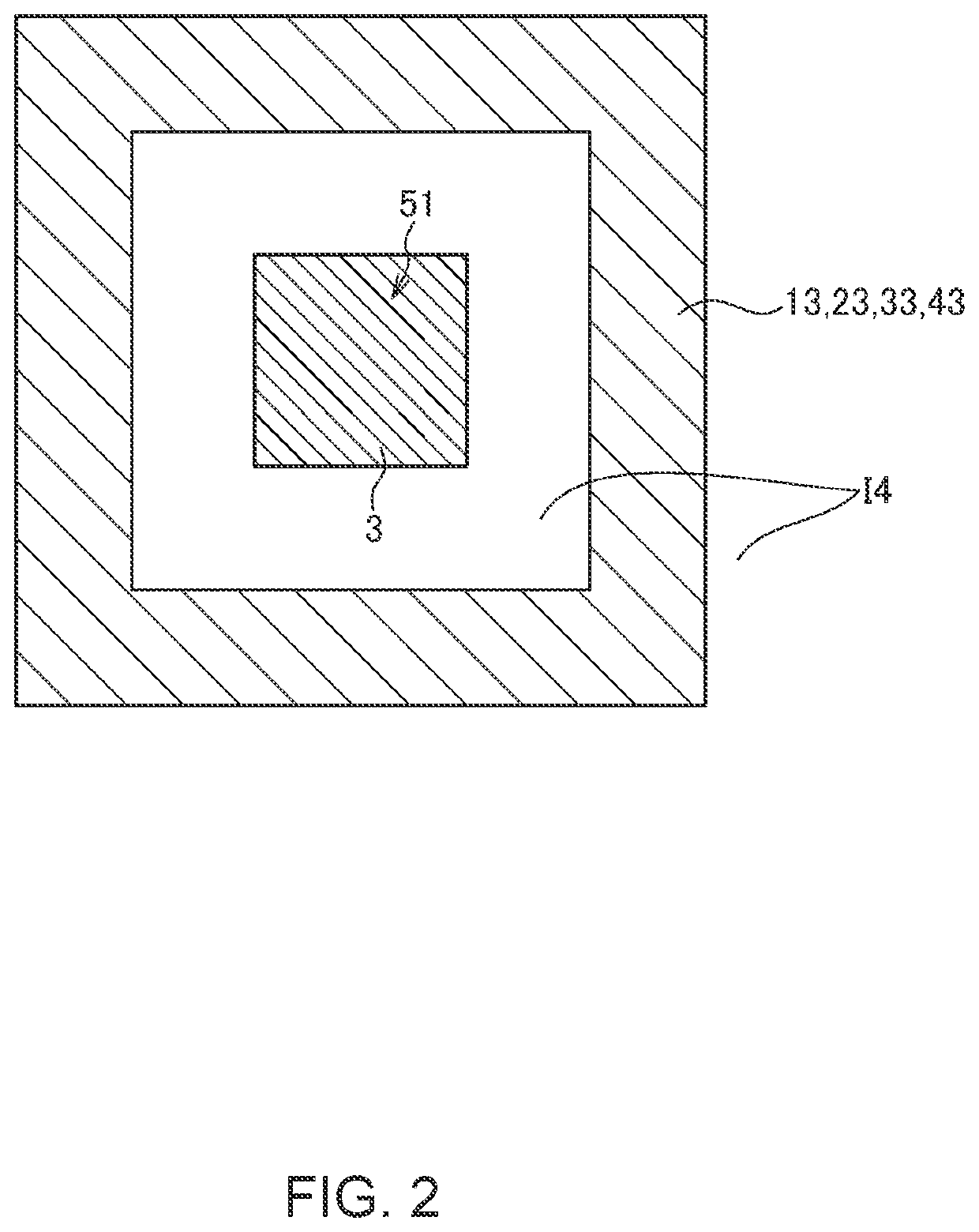
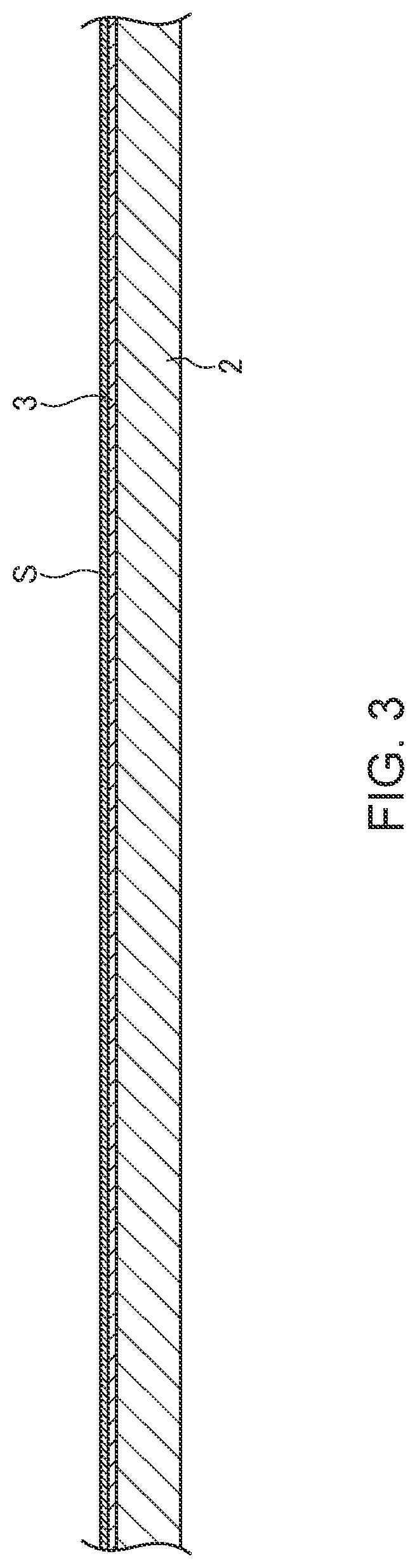
BRIEF DESCRIPTION OF THE DRAWINGS

[0025]Hereinafter, a preferred embodiment of the present invention will be described in detail with reference to the accompanying drawings.

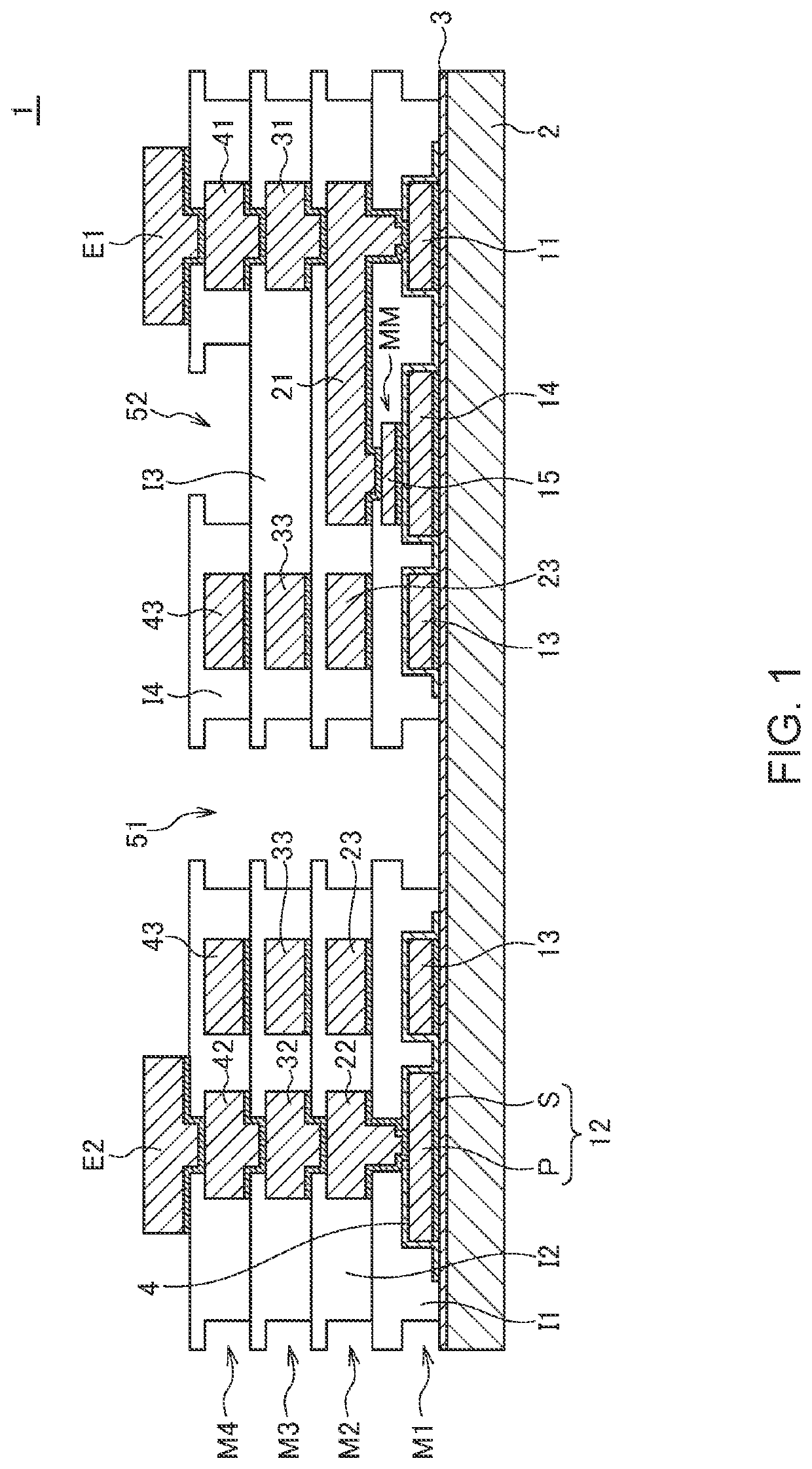
[0026]FIG. 1 is a cross-sectional view for explaining the structure of an electronic component 1 according to an embodiment of the present invention.

[0027]The electronic component 1 according to the present embodiment is an LC filter and includes a substrate 2, conductive layers M1 to M4, and insulating layers I1 to I4 as illustrated in FIG. 1. The conductive layers M1 to M4 and insulating layers I1 to I4 are alternately laminated on the upper surface of the substrate 2. The material for the substrate 2 may be any material as long as it is chemically and thermally stable, generates less stress, and can maintain surface smoothness, and examples thereof include, but not particularly limited thereto, silicon single crystal, alumina, sapphire, aluminum nitride, MgO single crystal, SrTiO3 single crystal, surface-oxidiz...


PUM


Abstract

Disclosed herein is an electronic component that includes a substrate, a planarizing layer covering a surface of the substrate, a first conductive layer formed on the planarizing layer and having a lower electrode, a dielectric film made of a material different from that of the planarizing layer and covering the planarizing layer and first conductive layer, an upper electrode laminated on the lower electrode through the dielectric film, and a first insulating layer covering the first conductive layer, dielectric film, and upper electrode. An outer periphery of the first insulating layer directly contacts the planarizing layer without an intervention of the dielectric film.

Description

BACKGROUND OF THE INVENTIONField of the Invention[0001]The present invention relates to an electronic component and a manufacturing method thereof and, more particularly, to an electronic component having a capacitor and a manufacturing method thereof.Description of Related Art[0002]JP 2007-142109A and JP 2008-34626A disclose an electronic component having a capacitor and an inductor on a substrate. The capacitor described in JP 2007-142109A and JP 2008-34626A includes a lower electrode, a dielectric film that covers the lower electrode, and an upper electrode that faces the lower electrode through the dielectric film. In electronic components of such a type, a good conductor such as copper is used for the material of the upper and lower electrodes, and an inorganic insulating material such as silicon nitride is used for the dielectric film. The lower electrode is covered with an insulating layer made of an organic insulating material such as polyimide through the dielectric film. T...

Claims


Application Information

Patent Timeline
30 Dec 2021
Publication
US20210407737A1
IPC
H01G4/18; H01G4/40; H01G4/228
CPC
H01G4/18; H01G4/228; H01G4/40; H01G4/30; H01G4/33; H01F17/0013; H01G4/232; H01G4/385
Inventors
KUWAJIMA, HAJIME; OHTSUKA, TAKASHI