Manufacture of a curved electronic device using differential heating and curved electronic device

Pending Publication Date: 2022-01-13
NEDERLANDSE ORG VOOR TOEGEPAST-NATUURWETENSCHAPPELIJK ONDERZOEK (TNO)
View PDF0 Cites 0 Cited by
  • Summary
  • Abstract
  • Description
  • Claims
  • Application Information

AI Technical Summary

Benefits of technology

The present disclosure is about a method of making a curved electronic device. The method involves heating a substrate made of a thermoplastic material and then using a deformation process to create the desired shape of the device. This process ensures that the electronic components are protected from excess stress and damage during the curved shape transition. The technical effect of the method is that it allows for the production of curved electronic devices with improved reliability and stability.

Problems solved by technology

Especially at transitions between more and less thermoplastic materials, the strain can result in failure of electronic paths.
So friction and shear may occur which can result in risks for the integrity of the electronic system.
These measures may limit design freedom and are not always applicable.

Method used


Image

  • Manufacture of a curved electronic device using differential heating and curved electronic device
  • Manufacture of a curved electronic device using differential heating and curved electronic device
  • Manufacture of a curved electronic device using differential heating and curved electronic device

Examples


Embodiment Construction

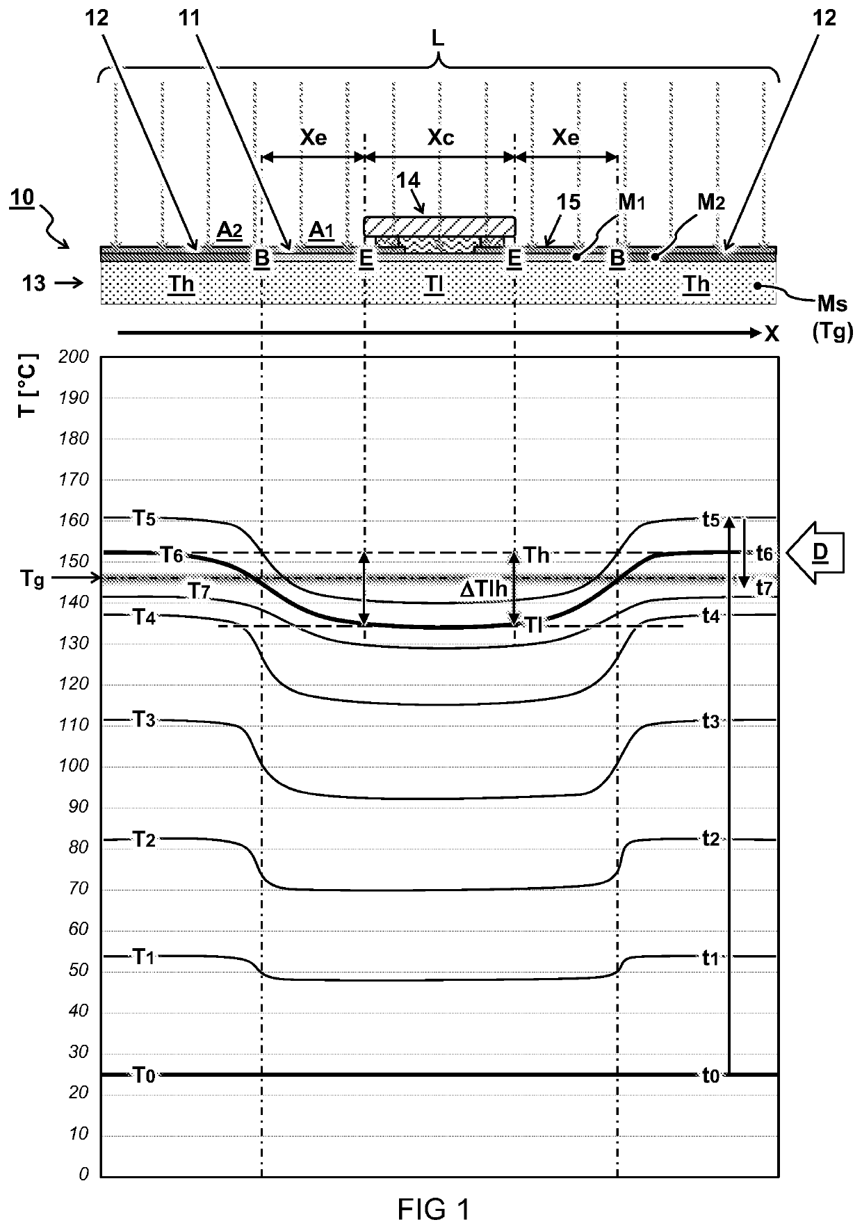
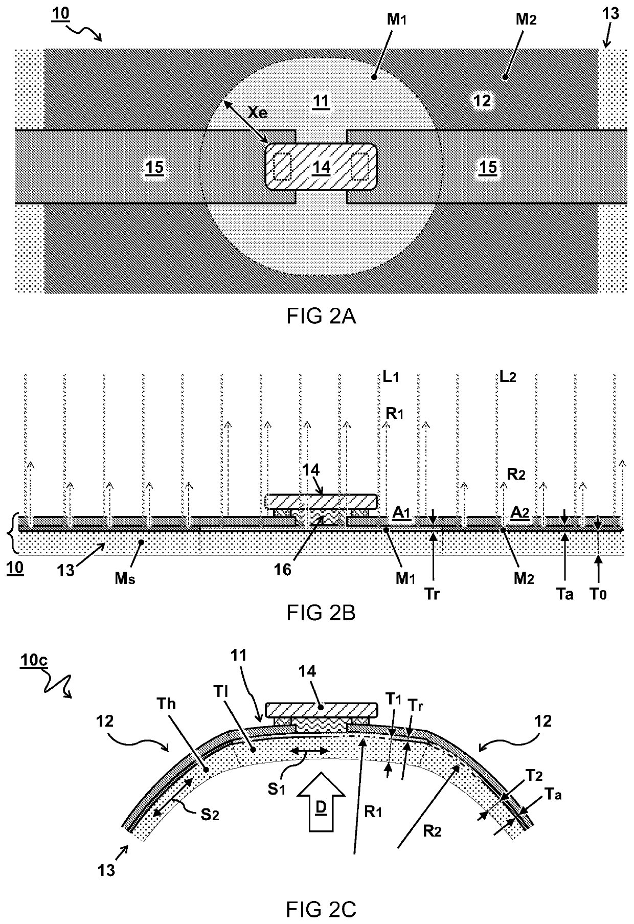
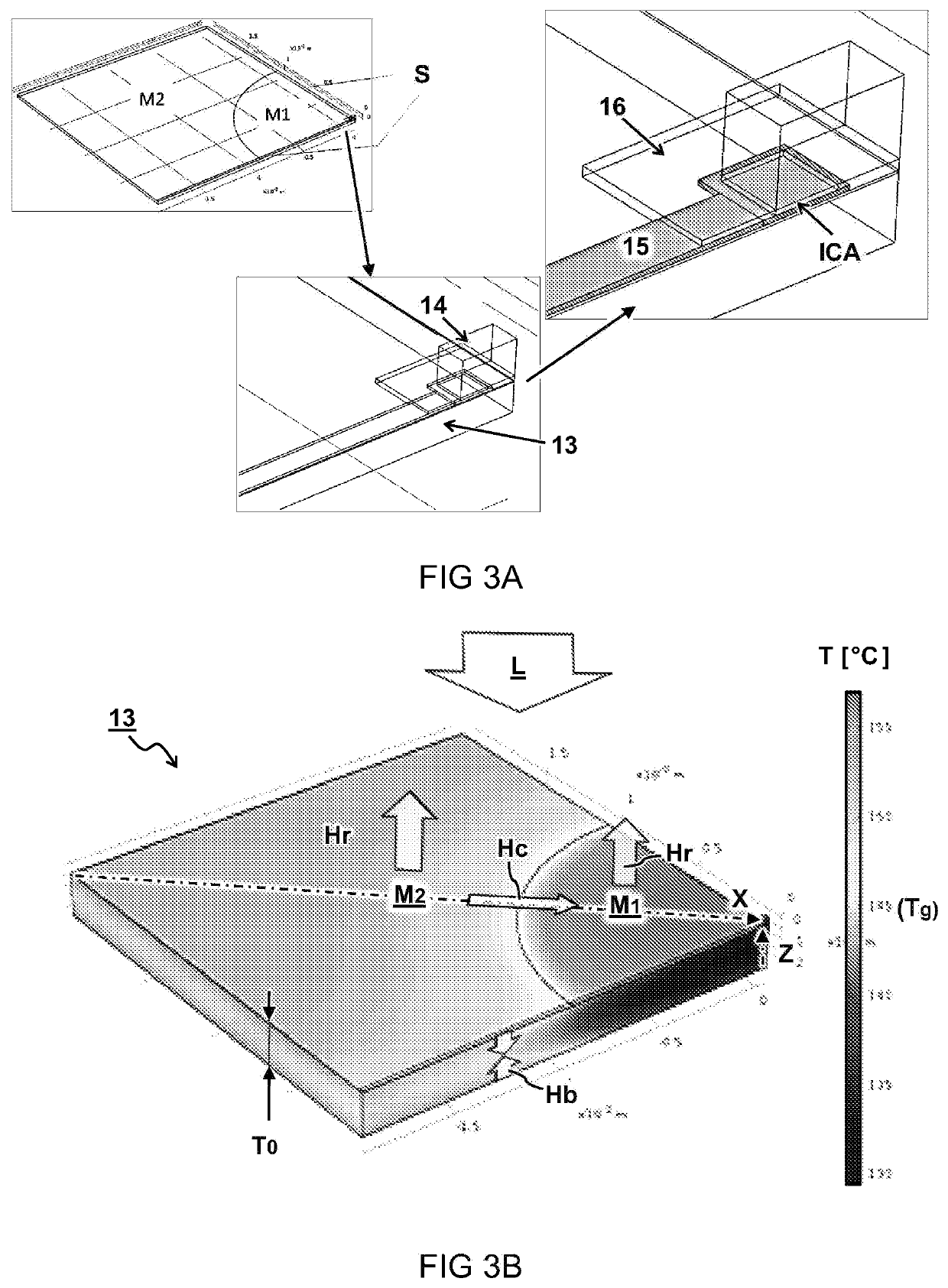
[0016]Terminology used for describing particular embodiments is not intended to be limiting of the invention. As used herein, the singular forms “a”, “an” and “the” are intended to include the plural forms as well, unless the context clearly indicates otherwise. The term “and / or” includes any and all combinations of one or more of the associated listed items. It will be understood that the terms “comprises” and / or “comprising” specify the presence of stated features but do not preclude the presence or addition of one or more other features. It will be further understood that when a particular step of a method is referred to as subsequent to another step, it can directly follow said other step or one or more intermediate steps may be carried out before carrying out the particular step, unless specified otherwise. Likewise it will be understood that when a connection between structures or components is described, this connection may be established directly or through intermediate stru...


PUM

PropertyMeasurementUnit
Fractionaaaaaaaaaa
Timeaaaaaaaaaa
Glass transition temperatureaaaaaaaaaa

Abstract

A curved electronic device (10c) can be formed by a stack with a curved substrate (13) comprising a thermoplastic material (Ms), and at least one electronic component (14) connected to an electronic circuit (15) disposed on the substrate (13). A component area (11) of the substrate surface (11.12) around the electronic component (14) comprises a first material (M1) providing relatively low absorption (A1) to light (L) and a surrounding area (12) of the substrate (13) outside the component area (11), comprises a second material (M2) providing relatively high absorption (A2) of the light (L). E.g. as a result of differential heating and thermoforming a first thickness (T1) of the substrate (13) in the component area (11) may be relatively high compared to a second thickness (T2) of the substrate (13) in the surrounding area (12).

Description

TECHNICAL FIELD AND BACKGROUND[0001]The present disclosure relates to methods of manufacturing curved electronic devices, and resulting products.[0002]Curved substrates can be manufactured e.g. using processes such as thermoforming. Thermoforming typically involves deformation of a material (stack) at elevated temperature. In case (printed) electronics are included in this composition deformation usually requires stretchability of all materials including the electronic. Especially at transitions between more and less thermoplastic materials, the strain can result in failure of electronic paths. Materials used in a stack may include e.g. a carrier (substrate) and electronic materials which are typically dissimilar with regards to their thermal behavior, plastic behavior and stretch behavior. So friction and shear may occur which can result in risks for the integrity of the electronic system.[0003]Various measures can be taken to alleviate the issue. For example, interconnects can be ...

Claims


Application Information

Patent Timeline
IPC IPC(8): H05K1/02B29C53/84H05K3/00
CPCH05K1/0284B29C53/84B29C53/04H05K3/0014H05K1/0274H05K1/0278H05K2201/0112H05K2201/0129H05K2201/0187H05K2201/0191H05K2201/0195H05K2201/09972H05K2201/2054H05K2203/1105H05K2203/1484H05K2203/1572H05K2203/1581H05K2203/304B29L2031/34H05K1/119B29B13/08
Inventor DE KOK, MARGARETHA MARIAKUSTERS, ROEL HENRY LOUISVAN DELFT, JAN PIETER HEINSCHRAM, JEROEN FRANCISCUS MARINUSVAN DER WAAL, ADRIRUBINGH, JAN-ERIC JACK MARTIJNVAN DEN BRAND, JEROEN
Owner NEDERLANDSE ORG VOOR TOEGEPAST-NATUURWETENSCHAPPELIJK ONDERZOEK (TNO)
Why Eureka
Try Eureka