Self-organized quantum dot manufacturing method and quantum dot semiconductor structure

a manufacturing method and quantum dots technology, applied in the field of self-organized quantum dots manufacturing methods, can solve the problems of difficult uniformity and reproducibility of inter-dot spacing, difficult to achieve placement precision of quantum dots, and difficulty in producing lithographically-patterned quantum dots with sufficiently small sizes, etc., to achieve high controllability and reproducibility, suitable for large-scale quantum computing device fabrication

Active Publication Date: 2022-01-20
NAT CHIAO TUNG UNIV
View PDF0 Cites 0 Cited by
  • Summary
  • Abstract
  • Description
  • Claims
  • Application Information

AI Technical Summary

Benefits of technology

The present invention is a method for producing quantum dots using existing CMOS manufacturing processes. The quantum dots can be tuned in terms of size and inter-dot spacing. The semiconductor structure can perform quantum transport at relatively high temperatures and the size of the quantum dots can be downsized to 5 nanometers or less. Additionally, the quantum dot manufacturing method is compatible with the existing CMOS manufacturing process. The invention also provides a paired quantum dot configuration where quantum dots are self-organizedly capped by silicon dioxide spacer islands and adhered to a conductive ridge, which is a portion of an electrode self-aligned to the corresponding quantum dot via the silicon dioxide spacer islands.

Problems solved by technology

The prior quantum dot manufacturing processes can be based on chemical synthesis, wherein the quantum dots have good size tunability, but the placement precision of quantum dots (especially the inter-dot spacing between quantum dots for quantum entanglement in quantum computing) is difficult, presenting a major challenge in making electrical contacts to specific QDs.
Or, the quantum dots can be formed by epitaxial growth, wherein the placement precision of quantum dots is still difficult to achieve.
Or else, lithography is another option for forming the quantum dots, but producing lithographically-patterned quantum dots with sufficiently small sizes and inter-dot spacings are difficult in terms of uniformity and reproducibility due to the resolution of lithography techniques (the current size resolution is about 10 nanometers by EUV).
In short, the prior quantum dot manufacturing methods are difficult for obtaining sufficiently small, closely-coupled quantum dots with placement precision, to let alone how to tune the size of (and spacing between) quantum dots in the manufacturing process.
Further, under the quantum dot nanometer size and placement requirement, after forming and placing the quantum dots, making electrical contacts to the quantum dots is also a challenge in such a high placement precision requirement.
Further, when nanoscale, closely-coupled quantum dots are formed laterally and vertically, making electrodes to specific quantum dots not only one-dimensional, but multiple-dimensional, which greatly increase the difficulty.
Besides the aforementioned problems of the prior quantum dot technology, the operation temperature of quantum dot devices, in particular for quantum computing devices, is another challenge.

Method used


Image

  • Self-organized quantum dot manufacturing method and quantum dot semiconductor structure
  • Self-organized quantum dot manufacturing method and quantum dot semiconductor structure
  • Self-organized quantum dot manufacturing method and quantum dot semiconductor structure

Examples


Embodiment Construction

[0016]The objectives, technical details, features, and effects of the present invention will be better understood with regard to the detailed description of the embodiments below, with reference to the drawings.

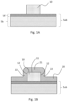
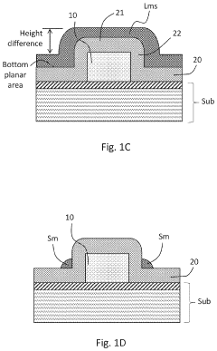
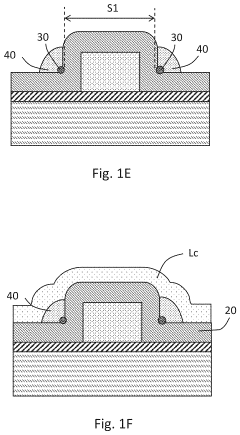
[0017]In one perspective, please refer to FIGS. 1A-1E, the present invention provides a quantum dot manufacturing method, which includes: forming a conductive ridge 10 (including a conductive material therein) on a substrate Sub (FIG. 1A); forming an insulative layer 20 to cover the substrate Sub and the conductive ridge 10 (FIG. 1B), wherein the insulative layer 20 is coated on the conductive ridge 10 to conformally form a top portion 21 on a top 11 of the conductive ridge 10 and two sidewalls 22 adhered to two sidewalls 12 of the conductive ridge 10; conformally forming a semiconductor-alloyed layer Lms over the insulative layer 20 (FIG. 1C), and etching back the semiconductor-alloyed layer Lms to form a plurality of semiconductor-alloyed spacer islands Sm separately adhere...


PUM

PropertyMeasurementUnit
sizeaaaaaaaaaa
temperatureaaaaaaaaaa
sizesaaaaaaaaaa

Abstract

The invention provides a quantum dot manufacturing method and related quantum dot semiconductor structure. The quantum dot semiconductor structure includes: a conductive ridge on a substrate; an insulative layer covering the substrate and the conductive ridge, wherein the insulative layer includes a top portion and two sidewalls over the conductive ridge; a plurality of quantum dots respectively embedded within a plurality of silicon dioxide spacer islands, which are adhered to the sidewalls of the insulative layer; and a plurality of conductive ledges adhered to the silicon dioxide spacer islands, wherein each of the conductive ledges is a portion of an electrode with alignment to the corresponding quantum dot.

Description

BACKGROUND OF THE INVENTIONField of Invention[0001]The present invention relates to a quantum dot manufacturing technology, especially a quantum dot manufacturing technology having tunable and self-aligned capability, and compatibility with CMOS manufacturing process.Description of Related Art[0002]Recently, semiconductor quantum dots (can be abbreviated as QDs) qubits have emerged as the subject of intensive research. The excellent properties of quantum dots have caused researchers and companies to consider using them in several fields for future development.[0003]Quantum dots are a few nanometers in size and their sizes are very critical for their electrical and optical properties. Quantum dots have electronic properties that differ from high dimensional materials due to quantum confinement. The prior quantum dot manufacturing processes can be based on chemical synthesis, wherein the quantum dots have good size tunability, but the placement precision of quantum dots (especially th...

Claims


Application Information

Patent Timeline
Patent Type & AuthorityApplications(United States)
IPC IPC(8): H01L21/02H01L21/308H01L29/12H01L29/165
CPCH01L21/02694H01L21/0259H01L21/02491H01L29/165H01L21/02532H01L21/3085H01L29/127H01L21/02488H01L29/66439H01L21/02494H01L21/02505H01L29/0665B82Y10/00H01L29/16
InventorLI, PEI-WENPENG, KANG-PINGCHEN, CHING-LUNHUANG, TSUNG-LIN
OwnerNAT CHIAO TUNG UNIV