Microstructure, method for manufacturing same, and molecule detection method using same

a microstructure and molecule technology, applied in the field of microstructure, can solve the problems of incompatibility with large micron-order objects, no indication of the specific application of fabricated microparticles in the field of life science, and no method has been shown for applications other than cell collection, so as to increase the sensitivity of signal detection, suppress background light noise, and high-sensitivity measurements

Pending Publication Date: 2022-01-27
NAT INST OF ADVANCED IND SCI & TECH
View PDF0 Cites 0 Cited by
  • Summary
  • Abstract
  • Description
  • Claims
  • Application Information

AI Technical Summary

Benefits of technology

[0028]In other words, the present invention provides a method of producing a hemispherical shell (or shell-shaped) microstructure, characterized by arrangement of electrodes on the concave side, made of a thin metal film of the thickness and diameter desired to be produced, and a method of detecting target biomolecules using the same. The present invention also provides a method for producing and controlling a microstructure in which the outer surface of the electrode microstructure described above includes a magnetic material and the orientation of the microstructure can be controlled by applying an external magnetic field, and a method for producing a magnetic microstructure described above by performing a mold particle removal reaction in an environment with a low oxygen concentration (e.g., less than about 15%), thereby providing the microstructure with high magnetic field responsiveness, a method of producing the microstructure in which the electrode material of the electrode microstructure above is a thin film of nanocarbon in which sp2 and sp3 binding regions are mixed and which can be formed on a curved surface, a method of capturing a biomolecule or cell inside the microstructure by orientating and arranging the electrode microstructure on a flat substrate, and a method of capturing a biomolecule or cell inside the microstructure using the electrode microstructure dispersed in a solution, and controlling the orientation of the microstructure by applying an external magnetic field.
[0030]The advantage of the microstructure of the present invention is that it can employ electrochemiluminescence for the detection of biomolecules, which eliminates the need for excitation light, suppresses background light noise, and enables highly sensitive measurements.
[0031]When the microstructure of the present invention is used to detect biomolecules by receiving a cell or biomolecules in the cavity on the concave side of the microstructure, the electrode can be placed in contact with a larger area of the cell surface compared to a conventional electrode placed on a flat substrate. The electrode can be placed in closer proximity to the electrochemiluminescent probes bound to the biomolecules expressed on the cell surface, which significantly increases the sensitivity of signal detection from the probes. In particular, when the microstructure of the present invention, which has a concave surface with a curved surface such as a hemispherical or semi-ellipsoidal shape, is used for the detection of biomolecules on the cell surface, the effect can be enhanced because the microstructure is shaped to better follow the curved surface of the cell surface.
[0032]The detection of biomolecules on the cell surface using the microstructures of the present invention makes it easier to detect signals from biomolecules on the cell surface, which were previously difficult to detect due to obstruction (or shielding) by the three-dimensional structure of the cell itself.
[0033]Applying an external magnetic field to the magnetic microstructure of the present invention makes it easier to control the orientation of the microstructure (e.g., orientation arrangement), and as a result, cells can be captured on the concave side of the microstructure in the solution phase first, which is expected to significantly improve the cell capture rate on the microstructure. In addition, since it is easier to attach the microstructure to the electrode surface after capturing cells in the solution phase, it is easier to apply a voltage to the microstructure, which in turn makes it easier to detect the cells or biomolecules received on the concave surface of the microstructure using a probe label.

Problems solved by technology
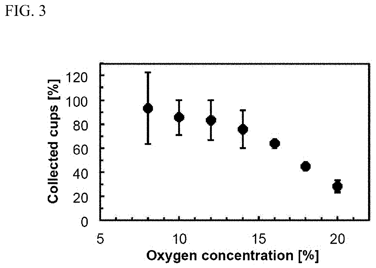
However, there is no indication of the specific application of the fabricated microparticles in the field of life science, especially the application of detecting biomolecules such as proteins and DNAs, which are important in medical diagnosis.
However, no method has been shown for applications other than cell collection, especially for identifying the type and nature of cells by detecting biomolecules expressed on the surface of the collected cells.
On the other hand, since ECL is a luminescence phenomenon that occurs only at a few nm near the electrode, it is incompatible with large micron-order objects such as cells, and there have been no research examples using cells as measurement targets.
However, because graphene is flat at the atomic level, constructing graphene films on curved microstructures with curvature requires technological innovation.
However, there have been no examples of deposition on three-dimensional materials such as hemispherical microstructures.

Method used


Image

  • Microstructure, method for manufacturing same, and molecule detection method using same
  • Microstructure, method for manufacturing same, and molecule detection method using same
  • Microstructure, method for manufacturing same, and molecule detection method using same

Examples


Embodiment Construction

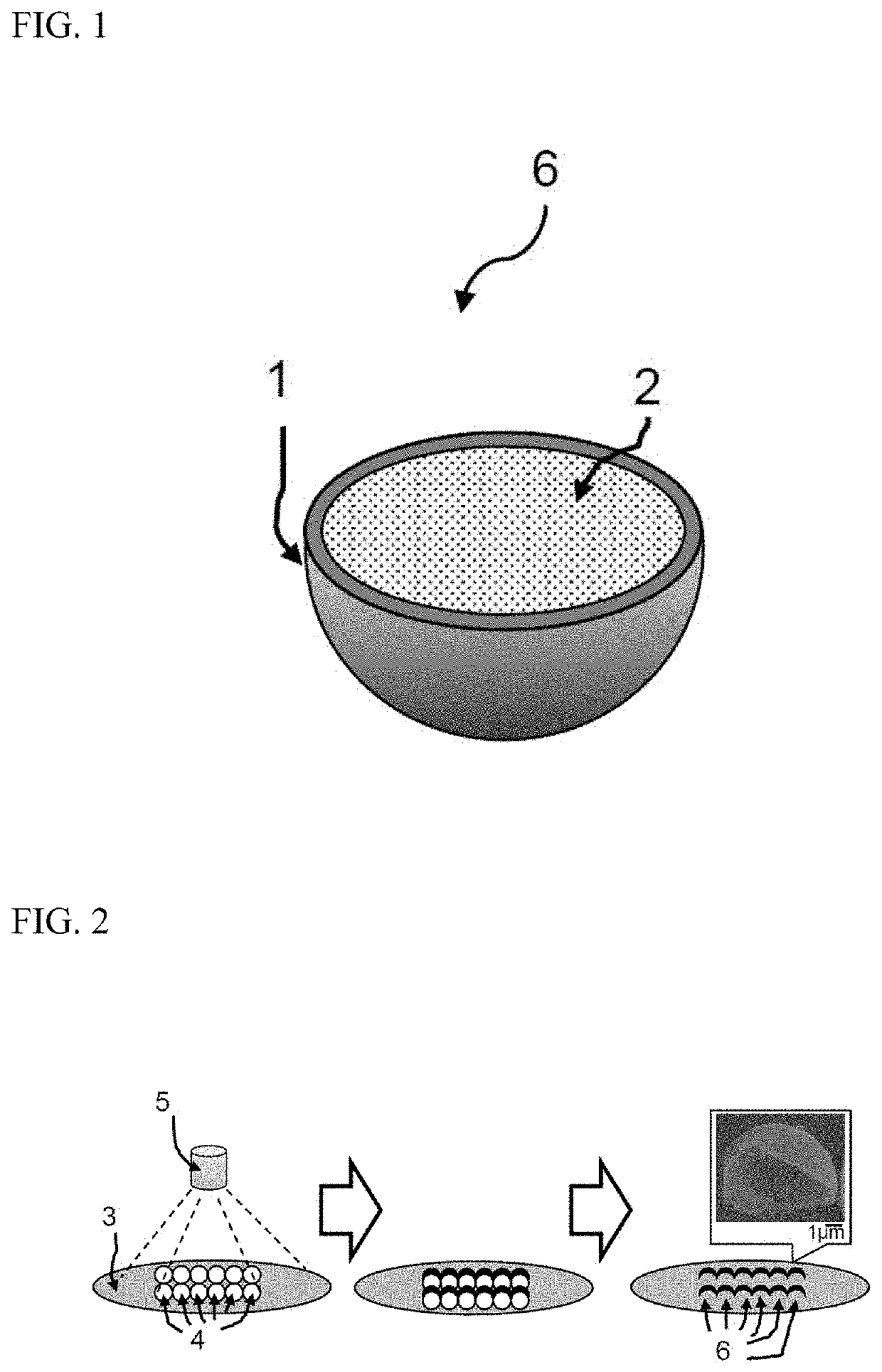
1. Microstructures for Use in the Detection of Molecules

[0041]In one aspect, the present invention provides microstructures for use in the detection of molecules (sometimes referred to herein as “microstructures of the present invention” or “electrode microstructures,”“hemispherical shell-shaped microstructures,” etc.). In one typical embodiment, the first conductive material includes a magnetic material, and the second conductive material includes an electrode material.

[0042]Examples of the first conductive material include, but are not limited to, magnetic materials such as metals such as nickel, iron, and cobalt, oxides such as iron oxide and chromium oxide, or alloys such as ferrite and neodymium.

[0043]With respect to the present invention, when referring to “magnetic material,” the term “magnetic material” is used in its ordinary meaning as used in the art. For the purpose of the present invention, at least the “magnetic material” used in the present invention should be magneti...


PUM

PropertyMeasurementUnit
diameteraaaaaaaaaa
diameteraaaaaaaaaa
thicknessaaaaaaaaaa

Abstract

In order to provide a specific solution for producing a microstructure equipped with a mechanism for selectively detecting a marker molecule expressed by a target cell, or a specific biomolecule, and for detecting and identifying a molecule to be detected using the microstructure, the present invention provides a nearly hemispherical shell-shaped structure made of a first conductive material, and an electrode layer made of a second conductive material disposed on the concave side of the nearly hemispherical shell-shaped structure, wherein the first conductive material includes a magnetic material and the second conductive material includes an electrode material, and the size (diameter) of the cavity surrounded by the electrode layer on the concave side of the nearly hemispherical shell-shaped structure is in the range of about 10 nm to about 50 μm.

Description

TECHNICAL FIELD[0001]The present invention relates to microstructures with structures such as hemispherical shells and semi-ellipsoidal shells, which are comprised of an adhesive material of a metal thin film and a conductive electrode thin film, and a method of detecting substances using the microstructures.BACKGROUND ART[0002]Microstructures such as microparticles are widely used as materials for developing materials with novel physical properties, and as labeling materials for visualizing target proteins and DNAs in the life science field. Generally, spherical microparticles are widely used because they are easy to fabricate, but microparticles with complex shapes such as elliptical and polygonal microparticles have a wide range of applications because they have anisotropic optical properties.[0003]In Japanese Patent Application Publication No. 2011-101941, “Hollow Microbody and Method for Producing The Same” (Patent Document 1), a method for producing hemispherical shell micropa...

Claims


Application Information

Patent Timeline
Patent Type & Authority Applications(United States)
IPC IPC(8): G01N33/543G01N21/66G01N33/574G01N33/553B22F1/00B22F1/18
CPCG01N33/54346G01N21/66B82Y35/00G01N33/54326G01N33/553G01N33/574B22F1/00C12M1/34B82Y30/00B22F1/18B82Y40/00
Inventor KIM, HYONCHOLKATO, DAIKOJIMA, NAOSHIYAMAMURA, SHOHEIKAMATA, TOMOYUKI
Owner NAT INST OF ADVANCED IND SCI & TECH
Why Eureka
Try Eureka