Blankmask with backside conductive layer, and photomask manufactured with the same

Pending Publication Date: 2022-03-03
S & S TECH
View PDF7 Cites 0 Cited by
  • Summary
  • Abstract
  • Description
  • Claims
  • Application Information

AI Technical Summary

Benefits of technology

This patent is about a special blankmask with a layer of conductive material that has low resistance, strong adhesion to a surface, and low stress on the surface. This makes it easier to create and use the blankmask for various applications.

Problems solved by technology

When the sheet resistance is high, there is a risk of dielectric breakdown because it is necessary to apply a high voltage to obtain high adhesion to the electronic-chuck.
When the adhesion to the conductive layer 120 is low, there may be a problem in that alignment deteriorates as the blankmask slides during chucking.

Method used


Image

  • Blankmask with backside conductive layer, and photomask manufactured with the same

Examples


example 1

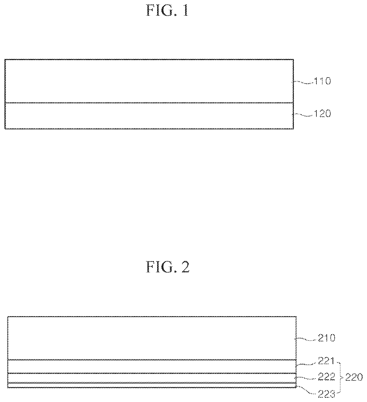
[0047]A conductive layer having a three-layer structure mainly made of Cr was formed on a backside of a SiO2-TiO2-based transparent substrate using DC magnetron reactive sputtering equipment. All of the first to third layers of the conductive layer were formed using a Cr target.

[0048]The first layer was formed of a CrCON film having a thickness of 41 nm by injecting Ar:N2:CO2=6 sccm:10 sccm:6 sccm as a process gas and using a process power of 1.4 kW. The second layer was formed of a CrCN film having a thickness of 30 nm by injecting Ar:N2:CH4=5 sccm:5 sccm:0.8 sccm as a process gas and using a process power of 1.0 kW. The third layer was formed of a CrCON film having a thickness of 9 nm by injecting Ar:N2:CO2=3 sccm:5 sccm:7.5 sccm as a process gas and using a process power of 1.4 kW.

[0049]As a result of measuring a sheet resistance of the conductive layer using a 4-point probe, a sheet resistance value was shown as 15.6 Ω / □, and when a surface roughness was measured by atomic force...

example 2

[0056]In Example 2, a composition of a second layer of a conductive layer was changed from CrCN to CrN. In order to form the second layer, a CrN film having a thickness of 32 nm was formed by injecting Ar:N2=5 sccm:5 sccm as a process gas and using a process power of 1.0 kW. Other processes are the same as in Example 1. As a result of measuring a sheet resistance of the conductive layer using a 4-point probe, a sheet resistance value was shown as 20.2 Ω / □, and when a surface roughness was measured by atomic force microscope (AFM), a surface roughness value was shown as 0.28 nm RMS. Therefore, it was confirmed that there is no problem in bonding with the electronic-chuck and there is no problem in using the conductive layer of Example 2 as the conductive layer.

[0057]When the flatness of the conductive layer was measured with a flatness meter, the value of 190 nm was obtained, and the stress was compressive stress. The flatness of the front side of the substrate after the process of f...

example 3

[0058]In Example 3, a composition of a first layer was changed from CrCON to CrCO. In order to form the first layer, a CrCO film having a thickness of 39 nm was formed by injecting Ar:CO2=6 sccm:6 sccm as a process gas and using a process power of 1.4 kW Other processes are the same as in Example 1. As a result of measuring a sheet resistance of a conductive layer using a 4-point probe, a sheet resistance value of 21.6 Ω / □ was shown, and when a surface roughness was measured by atomic force microscope (AFM), a surface roughness value of 0.27 nm RMS was shown. Therefore, it was confirmed that there is no problem in bonding with the electronic-chuck and there is no problem in using the conductive layer of Example 3 as the conductive layer.

[0059]When the flatness of the conductive layer was measured with a flatness meter, the value of 190 nm was obtained, and the stress was compressive stress. The flatness of the front side of the substrate after the process of forming the absorbing fi...


PUM


Abstract

A blankmask includes a conductive layer attached to a backside of a substrate, and the conductive layer includes a first layer, a second layer, and a third layer that are sequentially stacked on the backside of the substrate. The first layer and the third layer are made of a material that contains chromium (Cr) and oxygen (O), and the second layer is made of a material that does not contain the oxygen (O) but contains the chromium (Cr). There is provided the blankmask with the conductive layer having characteristics of low sheet resistance, high adhesion to the substrate, and low stress applied to the substrate.

Description

CROSS-REFERENCE TO RELATED APPLICATION[0001]This application is based on and claims priority under 35 U. S. C. § 119 to Korean Patent Application No. 10-2020-0111761, filed on Sep. 2, 2020, the disclosure of which is herein incorporated by reference in its entirety.BACKGROUND1. Field[0002]The disclosure relates to a blankmask and a photomask, and more particularly, to a blankmask with a conductive layer on a backside of a substrate and a photomask manufactured with the same.2. Discussion of Related Art[0003]A blankmask has a structure in which various kinds of thin films are stacked on a substrate. Any kind of blankmask, for example, a reflective blankmask for extreme ultraviolet (EUV) has a conductive layer on a backside of a substrate. FIG. 1 is a side cross-sectional view of a conventional blankmask.[0004]The blankmask includes a substrate 110, various kinds of thin films (not illustrated) such as a reflection film and an absorbing film formed on a front side of the substrate 110...

Claims


Application Information

Patent Timeline
IPC IPC(8): G03F1/24H01L21/033
CPCG03F1/24H01L21/0332H01L21/0337G03F1/38G03F1/40G03F1/22
Inventor SEO, GYEONG-WONKONG, GIL-WOOYANG, CHUL-KYU
Owner S & S TECH
Why Eureka
Try Eureka