Formation of micro rough polysurface for low sheet resistant salicided sub-quarter micron polylines

Inactive Publication Date: 2006-01-31
STMICROELECTRONICS SRL
View PDF27 Cites 5 Cited by
  • Summary
  • Abstract
  • Description
  • Claims
  • Application Information

AI Technical Summary

Benefits of technology

[0008]An object of the invention is to provide a method for manufacturing a semiconductor device having low sheet resistance silicide over polysilicon lines of sub-quarter μm or eve

Problems solved by technology

However, although polysilicon provides many advantages, such as self-alignment, over metal as the gate material, its resistance level is still too high to provide interconnections among semiconductor devices.
As the size of semiconductor devices becomes smaller and smaller, how to provide good quality interconnections for devices having sub-quarter μm width of polysilicon lines becomes one of the major challenge to the current semiconductor industry.
Although polysilicon has a low contact resistance with silicon, it still exhibits too high a resistance to the interconnection metal materials.
The silicide film makes a low contact resistance with polysilicon and reduces the overall sheet resistance of the polycide structure.
Th

Method used


Image

  • Formation of micro rough polysurface for low sheet resistant salicided sub-quarter micron polylines
  • Formation of micro rough polysurface for low sheet resistant salicided sub-quarter micron polylines
  • Formation of micro rough polysurface for low sheet resistant salicided sub-quarter micron polylines

Examples


Example

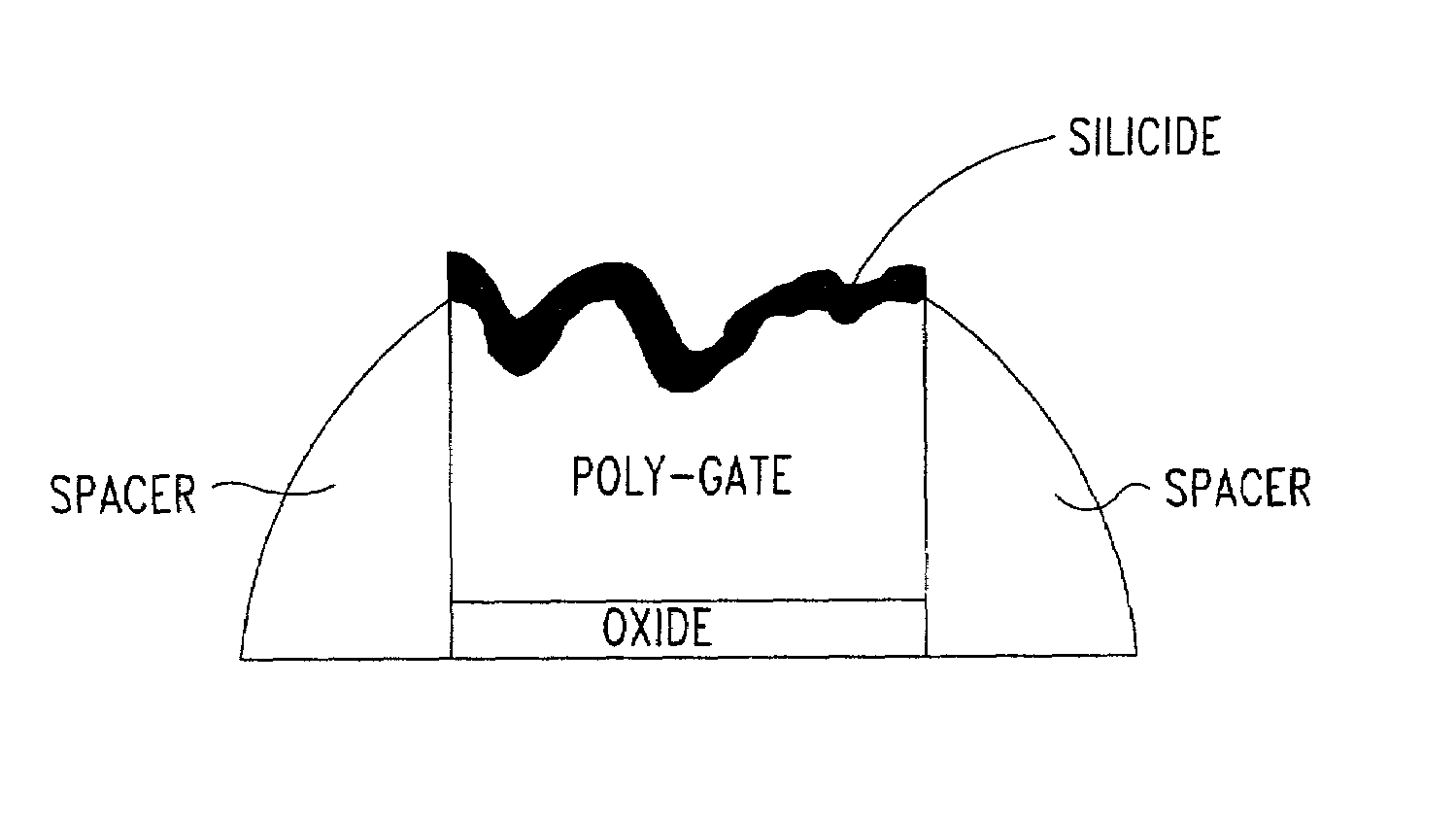
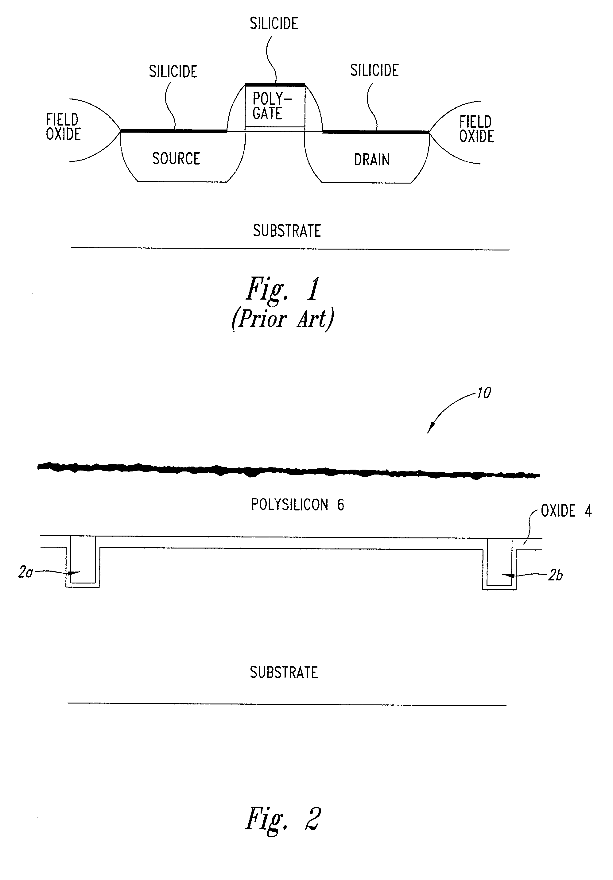
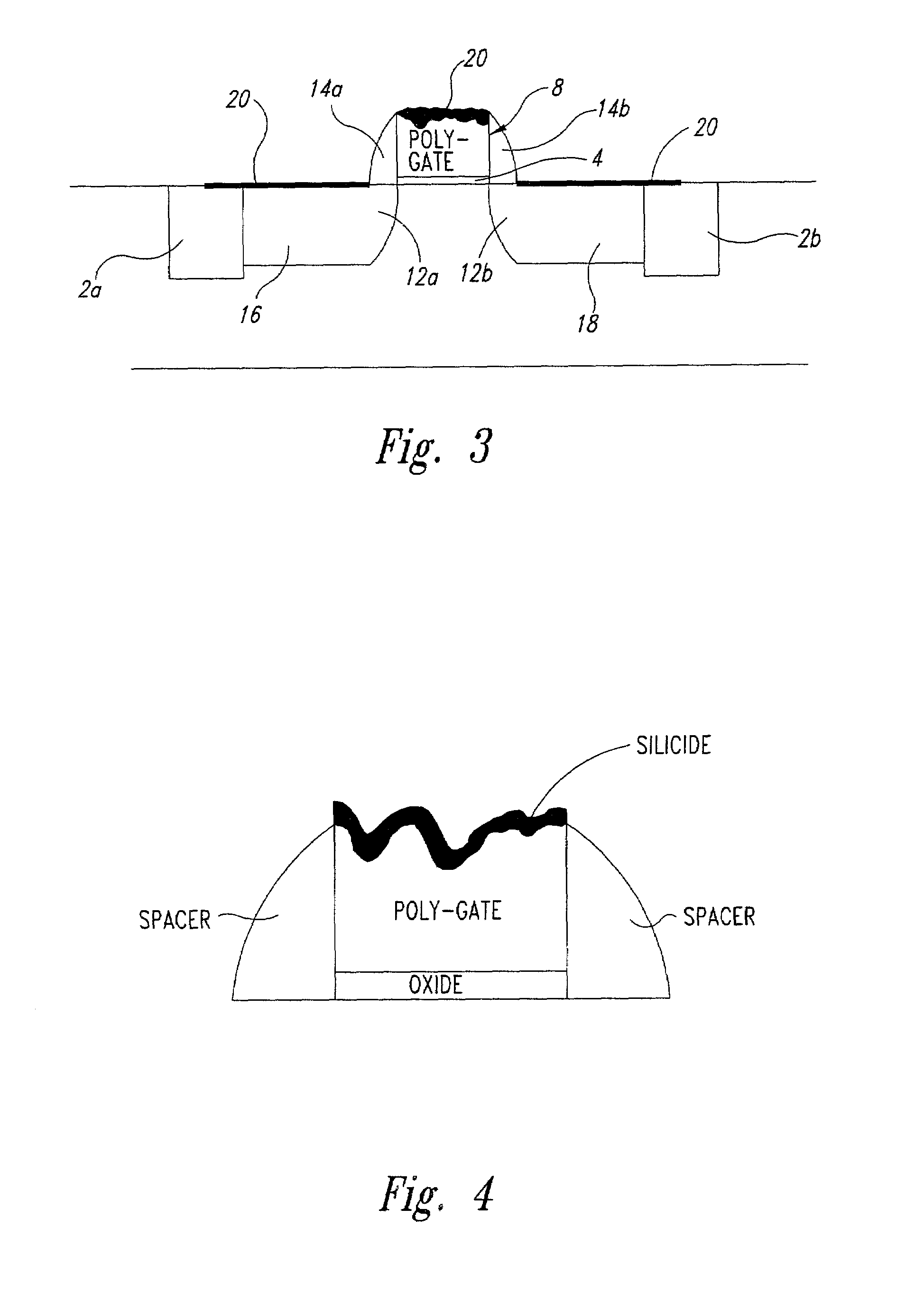
[0014]Referring to FIG. 2, an electrical isolation step is first performed on a semiconductor wafer 1 to isolate a device 10 from other devices of an integrated circuit. The isolation step may be accomplished by any suitable technology, such as the shallow trench isolation (STI), etch and back fill trench, or the LOCOS technology, trench being preferred over LOCOS. Isolation regions 2a and 2b are thus formed as shown in FIG. 2. After that, a gate oxide film 4 and then a polysilicon layer 6 are subsequently formed on the substrate. The polysilicon layer may be deposited by any suitable conventional technology, such as CVD or LPCVD. Typically, the polysilicon layer has a thickness of about 2000 Å–3000 Å, i.e., about 0.2 μm–0.3 μm.

[0015]After the polysilicon layer 6 is formed, a step for forming a micro-rough top surface of the polysilicon layer is carried out. The formation of a micro-rough top surface of the polysilicon layer 6 is accomplished by creating intentional scratches produc...


PUM


Abstract

This invention relates to a method for manufacturing a semiconductor device having polysilicon lines with micro-roughness on the surface. The micro-rough surface of the polysilicon lines help produce smaller grain size silicide film during the formation phase to reduce the sheet resistance. The micro-rough surface of the polysilicon lines also increases the effective surface area of the silicide contacting polysilicon lines thereby reduces the overall resistance of the final gate structure after metallization.

Description

CROSS-REFERENCE TO RELATED APPLICATION[0001]This application is a Divisional of U.S application Ser. No. 09 / 126,960, now U.S. Pat. No. 6,383,905 B2, filed Jul. 31, 1998.TECHNICAL FIELD[0002]This invention relates to a method for forming silicide on a polysilicon line of a semiconductor device. More particularly, this invention relates to a method for forming silicide over a controllable micro-rough surface of a polysilicon line, and a device made by the same.BACKGROUND OF THE INVENTION[0003]Polysilicon has become the prevalent gate material of MOS devices for over a decade. In addition to MOS gates, uses of polysilicon in MOS or other semiconductor devices have also increased prominently. However, although polysilicon provides many advantages, such as self-alignment, over metal as the gate material, its resistance level is still too high to provide interconnections among semiconductor devices. Therefore, after the formation and patterning of a polysilicon layer to form polysilicon l...

Claims


Application Information

Patent Timeline
IPC IPC(8): H01L23/48H01L23/52H01L29/40H01L21/28H01L21/285H01L21/321H01L21/336H01L29/423H01L29/49
CPCH01L21/28052H01L21/28518H01L21/321H01L29/42376Y10S438/964H01L29/4933H01L29/665
Inventor LI, MING MICHAEL
Owner STMICROELECTRONICS SRL
Why Eureka
Try Eureka