Semiconductor power module

a technology of semiconductor power modules and power electronics, applied in semiconductor devices, semiconductor/solid-state device details, electrical apparatus, etc., can solve the problems of large installation space requirements of power electronics for hybrid electric vehicles or electric vehicles, increased electrical losses, and high electrical properties. , to achieve the effect of improving cooling connection and increasing the distance between the two parallel power transistors

Pending Publication Date: 2022-03-10
ROBERT BOSCH GMBH
View PDF0 Cites 0 Cited by
  • Summary
  • Abstract
  • Description
  • Claims
  • Application Information

AI Technical Summary

Benefits of technology

[0005]A semiconductor power module in accordance with an example embodiment of the present invention may have the advantage that the effective inductances and ohmic resistances of the two power transistors situated in parallel between a first collector strip conductor and a first emitter strip conductor are adapted to one another via a particular line routing. This results in symmetrical control voltages at the two parallel power transistors, and in uniform switching on and switching off, so that the energy input is equally distributed over the two parallel power

Problems solved by technology

The power electronics for hybrid electric vehicles or electric vehicles together with associated semiconductor power modules are increasingly subject to large installation space requirements, as the result of which the semiconductor power modules together with electrical supply lines have smaller designs.
However, smaller supply lines and higher currents result in greater electri

Method used


Image

  • Semiconductor power module
  • Semiconductor power module
  • Semiconductor power module

Examples


Embodiment Construction

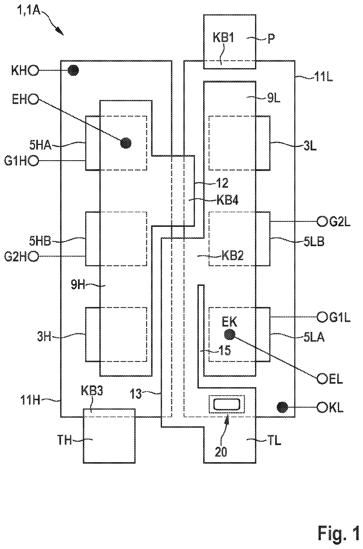
[0020]As is apparent from FIGS. 1 and 3, the illustrated exemplary embodiment of a semiconductor power module 1 according to the present invention includes a first power transistor 5LA and a second power transistor 5LB that are situated in parallel between a first collector strip conductor 11L and a first emitter strip conductor 9L, in each case a first connection surface of power transistors 5LA, 5LB being electroconductively connected to first collector strip conductor 11L, and in each case a second connection surface of power transistors 5LA, 5LB being electroconductively connected to first emitter strip conductor 9L, so that a current flowing between first collector strip conductor 11L and first emitter strip conductor 9L is divided between the two power transistors 5LA, 5LB when power transistors 5LA, 5LB are each conductively connected via an applied control voltage. A first external power contact P is directly contacted with first collector strip conductor 11 at a first conta...


PUM


Abstract

A semiconductor power module including first and second power transistors situated in parallel between first collector and first emitter strip conductors. A first connection surface of each of the power transistors is electroconductively connected to the first collector strip conductor, and a second connection surface of each of the power transistors is electroconductively connected to the first emitter strip conductor, so that a current flowing between the first collector strip conductor and the first emitter strip conductor is divided between the power transistors when the power transistors are each conductively connected via an applied control voltage. A first external power contact is directly contacted with the first collector strip conductor at a first contact area, a second external power contact is contacted with the first emitter strip conductor at a second contact area via a first connecting element, and the second contact area is positioned asymmetrically between the power transistors.

Description

[0001]The present invention relates to a semiconductor power module that includes a first power transistor and a second power transistor that are situated in parallel between a first collector strip conductor and a first emitter strip conductor. A first connection surface of the power transistors is in each case electroconductively connected to the first collector strip conductor, and a second connection surface of the power transistors is in each case electroconductively connected to the first emitter strip conductor, so that a current flowing between the first collector strip conductor and the first emitter strip conductor is divided between the two power transistors when the power transistors are each conductively connected via an applied control voltage.BACKGROUND INFORMATION[0002]The power electronics for hybrid electric vehicles or electric vehicles together with associated semiconductor power modules are increasingly subject to large installation space requirements, as the re...

Claims


Application Information

Patent Timeline
IPC IPC(8): H01L25/07H01L23/367H01L23/495H01L23/498H01L25/18
CPCH01L25/072H01L23/367H01L25/18H01L23/49894H01L23/49562H01L23/49524H01L23/36H01L23/49575H01L2224/40137
Inventor LAUTENSACK, CHRISTIAN MARCKAISER, ALEXANDERHOMOTH, JAN
Owner ROBERT BOSCH GMBH
Why Eureka
Try Eureka