Display device and manufacturing method thereof
- Summary
- Abstract
- Description
- Claims
- Application Information
AI Technical Summary
Benefits of technology
Problems solved by technology
Method used
Image

Examples
example 1
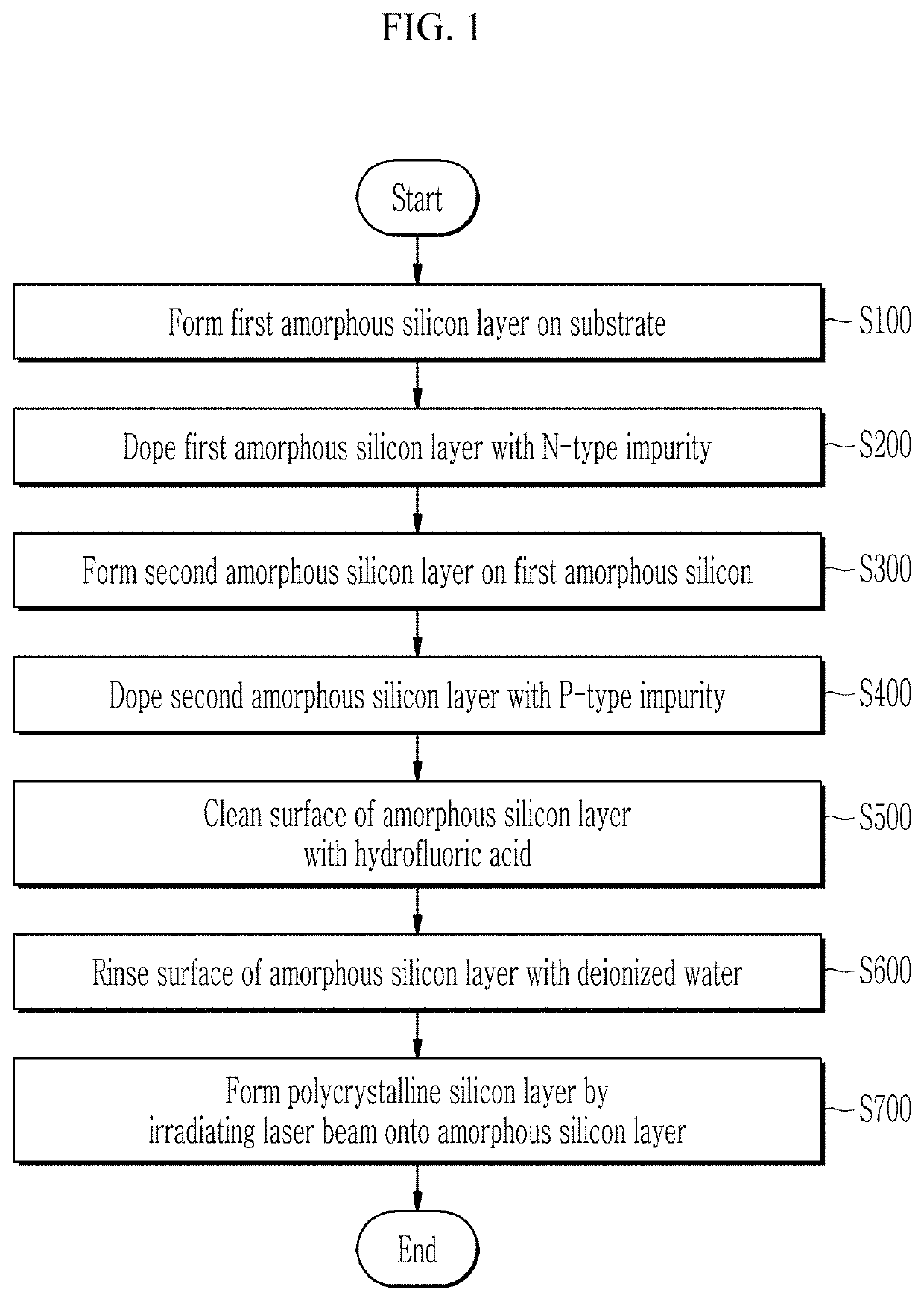
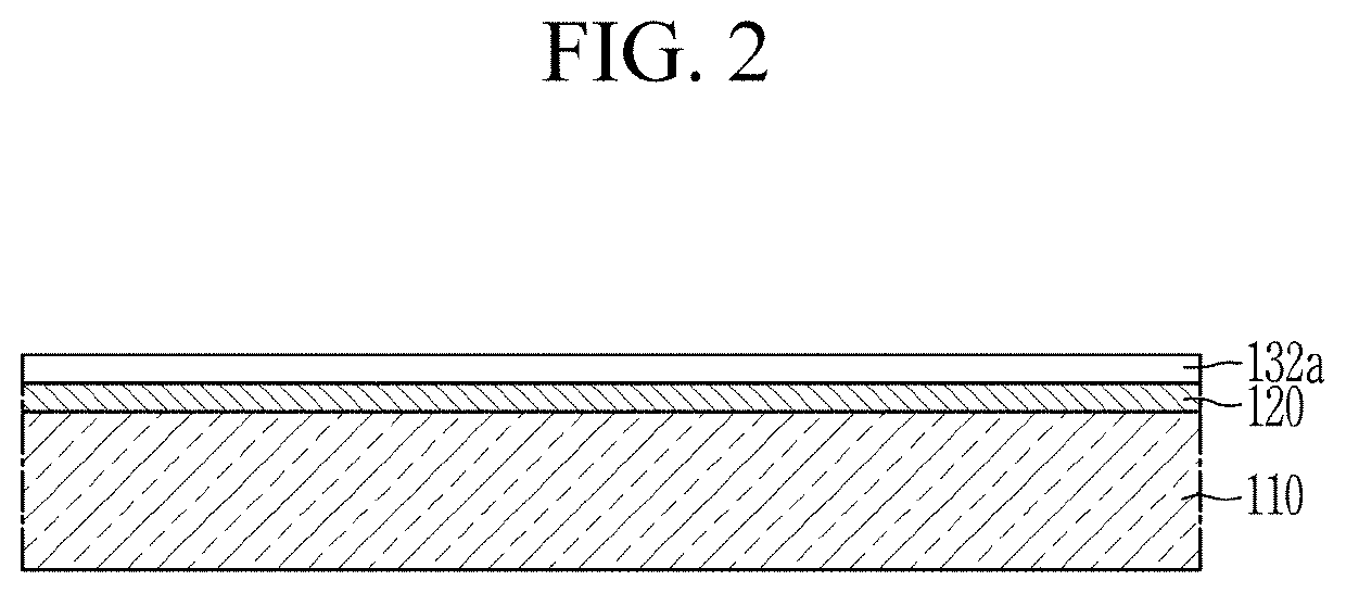
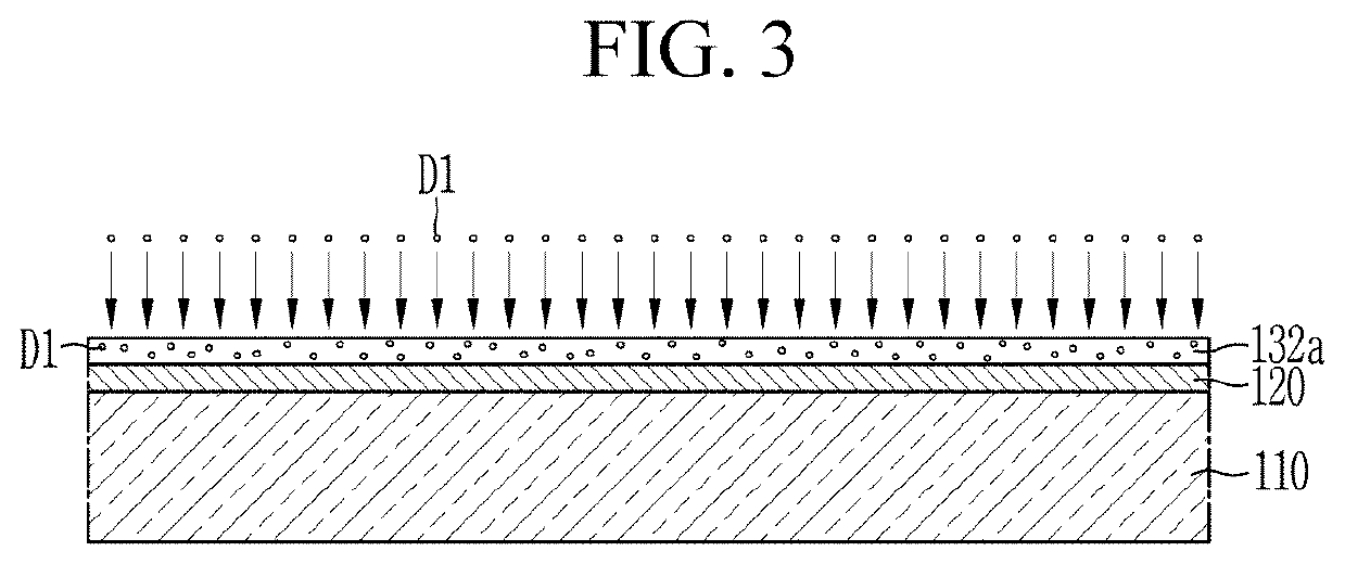
[0127]Sample doped with 1 e14 atoms / cm2 of phosphorus (P) on the first amorphous silicon layer and 1 e14 atoms / cm2 of boron (B) on the second amorphous silicon layer, and washed with hydrofluoric acid for 60 s.
[0128]Comparative Examples 2: Sample doped with 1 e12 atoms / cm2 of phosphorus (P) on the first amorphous silicon layer and 1 e12 atoms / cm2 of boron (B) on the second amorphous silicon layer, and washed with hydrofluoric acid for 60 s.
example 2
[0129]Sample doped with 1 e14 atoms / cm2 of phosphorus (P) on the first amorphous silicon layer and 1 e14 atoms / cm2 of fluorine (F) on the second amorphous silicon layer, and washed with hydrofluoric acid for 60 s.
PUM
 Abstract
Description
Claims
Application Information
 - R&D Engineer
- R&D Manager
- IP Professional
- Industry Leading Data Capabilities
- Powerful AI technology
- Patent DNA Extraction
Browse by: Latest US Patents, China's latest patents, Technical Efficacy Thesaurus, Application Domain, Technology Topic.
© 2024 PatSnap. All rights reserved.Legal|Privacy policy|Modern Slavery Act Transparency Statement|Sitemap