Method for preparing stacking structure, stacking structure and touch sensor
- Summary
- Abstract
- Description
- Claims
- Application Information
AI Technical Summary
Benefits of technology
Problems solved by technology
Method used
Image

Examples
embodiment 1
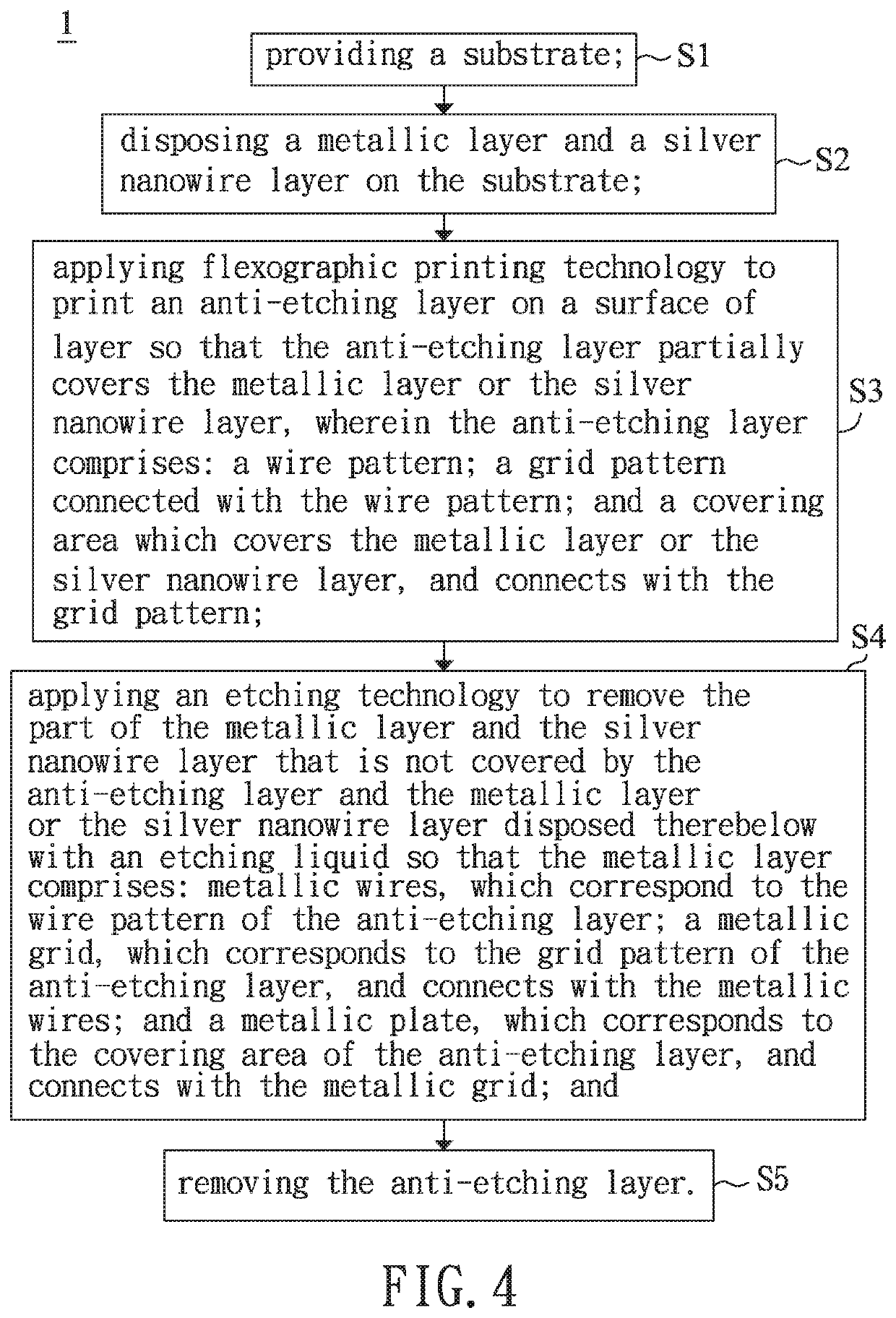
[0063]FIG. 4 is a flow sheet of a method 1 for preparing a stacking structure according to Embodiment 1 of the disclosure. As shown in FIG. 4, the method 1 for preparing a stacking structure according to Embodiment 1 of the disclosure comprises: S1, providing a substrate; S2, disposing a metallic layer and a silver nanowire layer on the substrate; S3, applying flexographic printing technology to print an anti-etching layer on a surface of the metallic layer or the silver nanowire layer so that the anti-etching layer partially covers the metallic layer or the silver nanowire layer, wherein the anti-etching layer comprises: a wire pattern; a grid pattern connected with the wire pattern; and a covering area which covers the metallic layer or the silver nanowire layer, and connects with the grid pattern; S4, applying an etching technology to remove the part of the metallic layer or the silver nanowire layer that is not covered by the anti-etching layer and the metallic layer or the silv...
embodiment 2
[0070]FIG. 6, FIG. 7 and FIG. 8 are schematic views of the stacking structure 20 of Embodiment 2 of the present disclosure. As shown in FIG. 6, FIG. 7 and FIG. 8, the stacking structure 20 of the embodiment comprises: a substrate 21 (not shown in FIG. 6); a metallic layer 22, which is disposed on the substrate 21, wherein the metallic layer 22 comprises: metallic wires 221; a metallic grid 222, which is connected to the metallic wires 221; and a metallic plate 223, which is connected to the metallic grid 222; and a silver nanowire layer 23, which is disposed on the substrate 21, wherein the silver nanowire layer 23 at least partially overlaps with the metallic layer 22.
[0071]The stacking structure 20 of the embodiment comprises: a trace area TA, which comprises the metallic wires 221; a first lap-over area 25, which comprises the metallic grid 222; a second lap-over area 26, which comprises the metallic plate 223; and a visible area VA, which comprises an area adjacent to one side o...
embodiment 3
[0091]FIG. 9, FIG. 10, FIG. 11 and FIG. 12 are schematic views of the stacking structure 30 of Embodiment 3 of the present disclosure. As shown in FIG. 9, FIG. 10, FIG. 11 and FIG. 12, the stacking structure 30 of the embodiment comprises: a substrate 31 (not shown in FIG. 9); a metallic layer 32, which is disposed on the substrate 31, wherein the metallic layer 32 comprises: metallic wires 321; a metallic grid 322, which is connected to the metallic wires 321; and a metallic plate 323, which is connected to the metallic grid 322; and a silver nanowire layer 33, which is disposed on the substrate 31, wherein the silver nanowire layer 33 at least partially overlaps with the metallic layer 32.
[0092]The stacking structure 30 of the embodiment comprises: a trace area TA, which comprises the metallic wires 321; a first lap-over area 35, which comprises the metallic grid 322; a second lap-over area 36, which comprises the metallic plate 323; and a visible area VA, which comprises an area ...
PUM
 Abstract
Description
Claims
Application Information
 - R&D Engineer
- R&D Manager
- IP Professional
- Industry Leading Data Capabilities
- Powerful AI technology
- Patent DNA Extraction
Browse by: Latest US Patents, China's latest patents, Technical Efficacy Thesaurus, Application Domain, Technology Topic.
© 2024 PatSnap. All rights reserved.Legal|Privacy policy|Modern Slavery Act Transparency Statement|Sitemap