Conductive via structure

a conductive via and structure technology, applied in the direction of semiconductor devices, electrical devices, semiconductor/solid-state device details, etc., can solve the problems of aluminum deposition efficiency decline, poor aluminum deposition efficiency, and poor electrical connection quality, so as to improve the electrical connection quality of the conductive via structure

Pending Publication Date: 2022-03-31
NAN YA TECH
View PDF12 Cites 2 Cited by
  • Summary
  • Abstract
  • Description
  • Claims
  • Application Information

AI Technical Summary

Benefits of technology

[0018]In the aforementioned embodiments, since the first width of the second dielectric layer is about 3 um to about 6 um greater than the second width of the second dielectric layer, clusters would not be formed at the top region of the opening during the aluminum deposition process. In other words, the portion of the redistribution layer 140 within the opening can be thicker. Therefore, the electrical connection quality of the conductive via structure can be improved.

Problems solved by technology

In the fabrication process of a redistribution layer through aluminum deposition, grands of aluminum may affect the efficiency of the subsequent process and the performance of the device.
Moreover, aluminum clusters may be formed at the top region of the opening, such that the aluminum deposition efficiency becomes worse.
As a result, the electrical connection quality may be degraded.
However, the greater size of the opening may limit the shrinkage level of the device.
As a result, the fabrication of a conductive via structure cannot obey the design rule.

Method used


Image

  • Conductive via structure
  • Conductive via structure
  • Conductive via structure

Examples


Embodiment Construction

[0026]Reference will now be made in detail to the present embodiments of the invention, examples of which are illustrated in the accompanying drawings. Wherever possible, the same reference numbers are used in the drawings and the description to refer to the same or like parts.

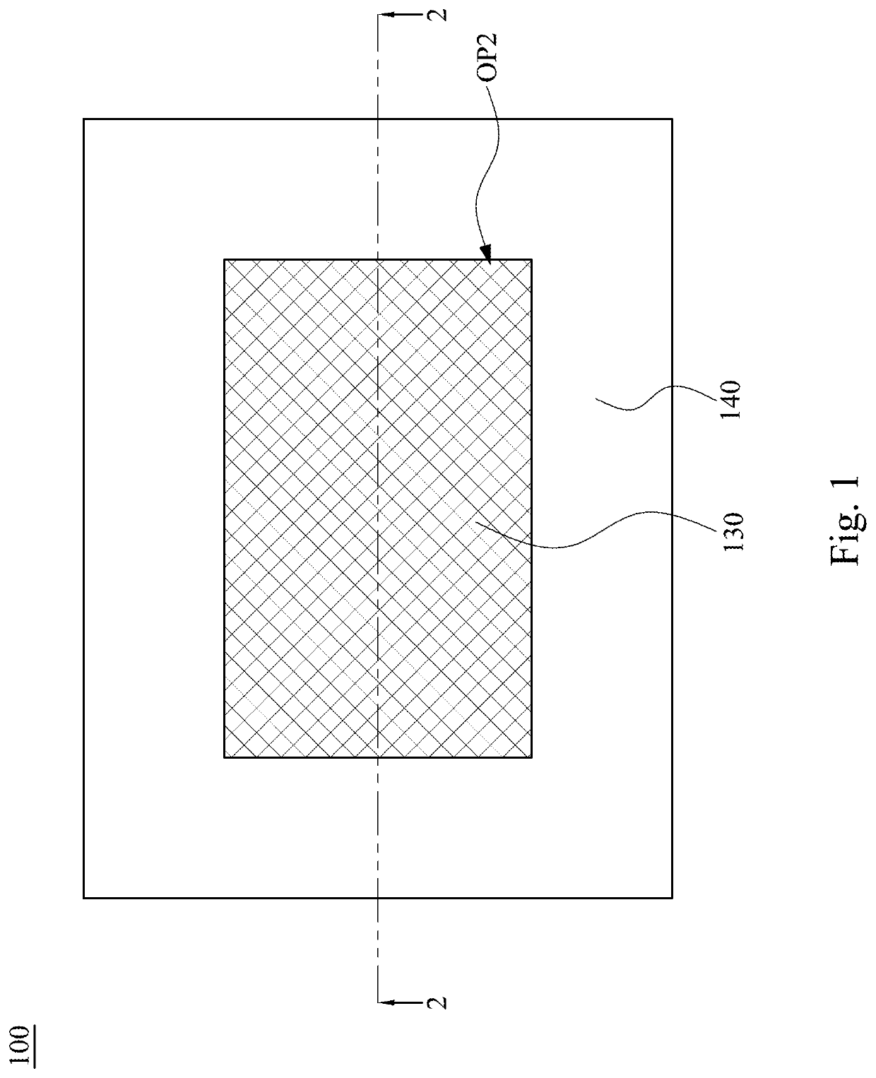
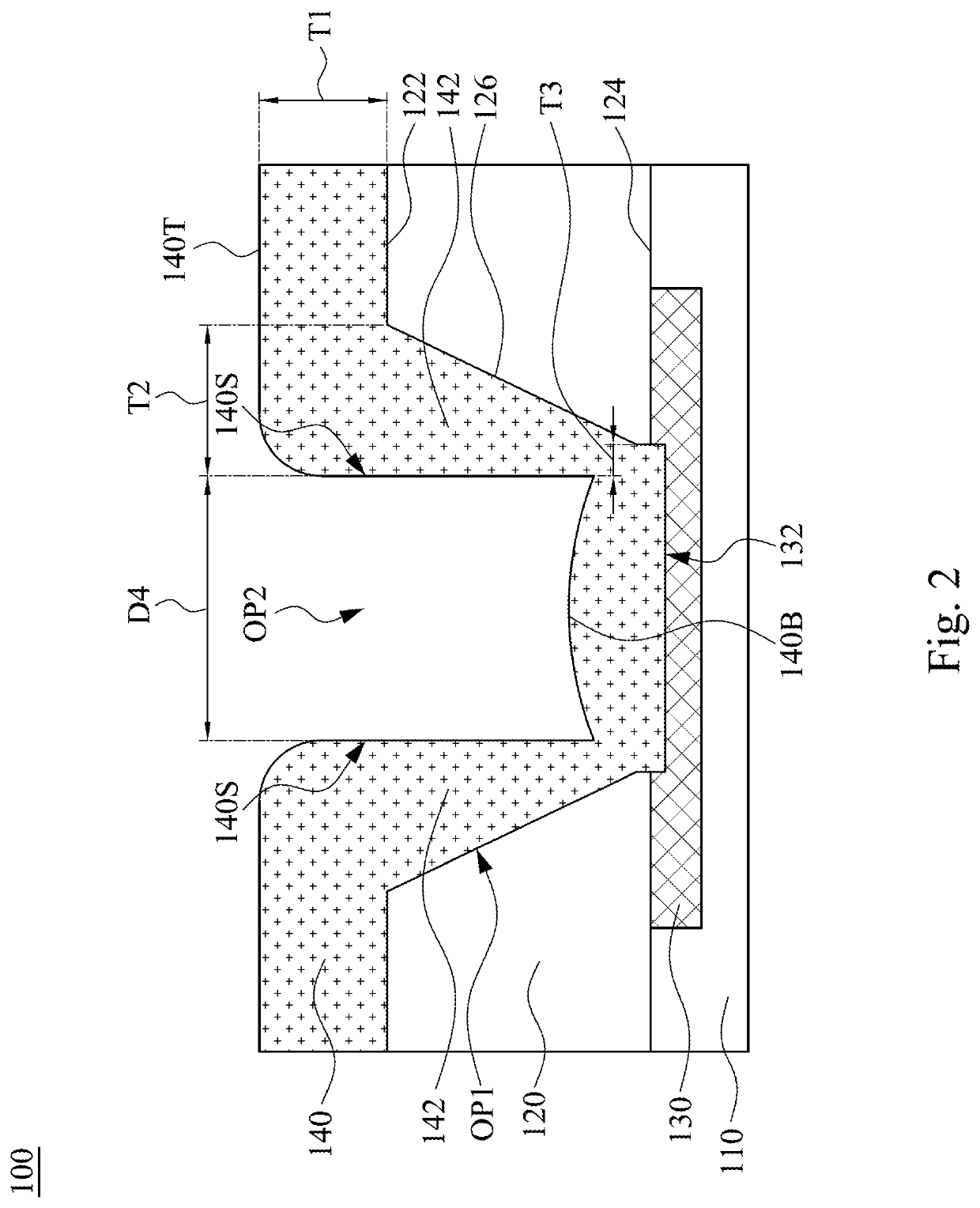
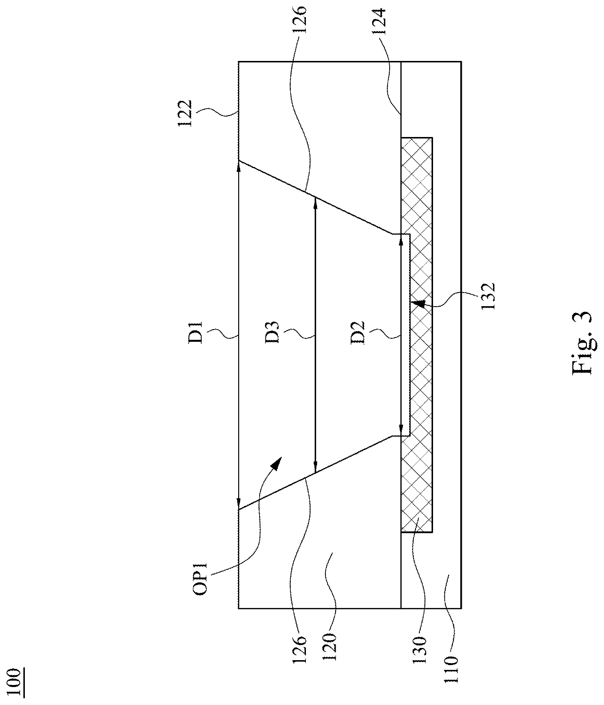
[0027]FIG. 1 is a top view of a conductive via structure 100 according to some embodiments of the present disclosure. FIG. 2 is a cross-sectional view of the conductive via structure 100 taken along line 2-2 shown in FIG. 1. Reference is made to FIGS. 1 and 2. The conductive via structure 100 includes a first dielectric layer 110, a second dielectric layer 120, a conductive pad 130, and a redistribution layer 140. In some embodiments, a substrate, such as a silicon substrate, a semiconductor substrate, or the like, may be located below the first dielectric layer 110 to support and electrically connect to the conductive pad 130. The conductive pad 130 is in the first dielectric layer 110. The second dielectric ...


PUM

PropertyMeasurementUnit
widthaaaaaaaaaa
widthaaaaaaaaaa
widthaaaaaaaaaa

Abstract

A conductive via structure includes a first dielectric layer, a conductive pad in the first dielectric layer, a second dielectric layer, and a redistribution layer. The second dielectric layer is disposed above the first dielectric layer and has an opening. The conductive pad is in the opening. The opening has a first width at a top surface of the second dielectric layer, a second width at a bottom surface of the second dielectric layer, and a third width between the top surface and the bottom surface of the second dielectric layer. A difference between the first and second width is in a range from about 3 um to about 6 um. The redistribution layer extends from the top surface of the second dielectric layer to the conductive pad. The third width is gradually decreased from the top surface to the bottom surface of the second dielectric layer.

Description

CROSS-REFERENCE TO RELATED APPLICATION[0001]The present application is a Divisional Application of the U.S. application Ser. No. 16 / 514,986, filed Jul. 17, 2019, the entirety of which is incorporated by reference herein in their entireties.BACKGROUNDField of Invention[0002]The present invention relates to a conductive via structure.Description of Related Art[0003]In the fabrication process of a redistribution layer through aluminum deposition, grands of aluminum may affect the efficiency of the subsequent process and the performance of the device. Therefore, in order to avoid formation of grains, the temperature of the aluminum deposition process may be lower. However, the lower temperature makes the thickness of the redistribution layer formed within the opening of the dielectric layer (for example, the conductive via) become thinner. Moreover, aluminum clusters may be formed at the top region of the opening, such that the aluminum deposition efficiency becomes worse. As a result, ...

Claims


Application Information

Patent Timeline
Patent Type & Authority Applications(United States)
IPC IPC(8): H01L21/48H01L23/538H01L23/29
CPCH01L21/486H01L23/291H01L23/5384H01L23/481H01L23/49827H01L23/5226H01L23/49894H01L23/53214H01L24/02H01L2224/0239H01L2224/0235H01L2224/0236H01L24/13H01L2224/13024H01L2224/024H01L2224/0231H01L2224/131H01L2924/01013H01L2924/059H01L2924/05042H01L2924/05442H01L2924/00012H01L2924/00014H01L2924/014
Inventor SHIH, SHING-YIH
Owner NAN YA TECH
Why Eureka
Try Eureka