
Method for implementing an integrated circuit comprising a random-access memory-in-logic

Pending Publication Date: 2022-05-12
XENERGIC AB
View PDF0 Cites 0 Cited by
  • Summary
  • Abstract
  • Description
  • Claims
  • Application Information

AI Technical Summary

Benefits of technology

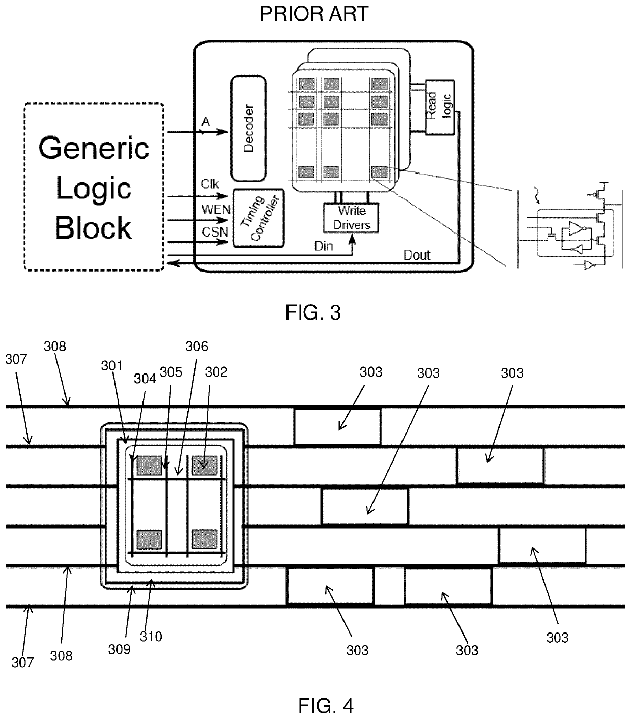
The present patent offers a method for combining the flexibility of multiple memory cells with the high efficiency of conventional RAMs. This is achieved by grouping memory cells into blocks that are compatible with standard cells, and distributing these blocks over the integrated circuit surface to optimize routing and bandwidth. The method provides higher bandwidth, energy efficiency, and more area-efficient memory design compared to standard cell memory. This solution is particularly useful for applications such as machine learning.

Problems solved by technology

At the same time there are increasing and to some extent conflicting requirements on area, access time, and power consumption.
This results in large RAM blocks.
Although the blocks are area efficient the limited number of ports (single or dual port) can result in memory bandwidth issues.
Also, these large RAM blocks cause routing and congestion issues.
However, standard cell memories have area penalty compared to bit cell based RAMs.

Method used


Image

  • Method for implementing an integrated circuit comprising a random-access memory-in-logic
  • Method for implementing an integrated circuit comprising a random-access memory-in-logic
  • Method for implementing an integrated circuit comprising a random-access memory-in-logic

Examples


Embodiment Construction

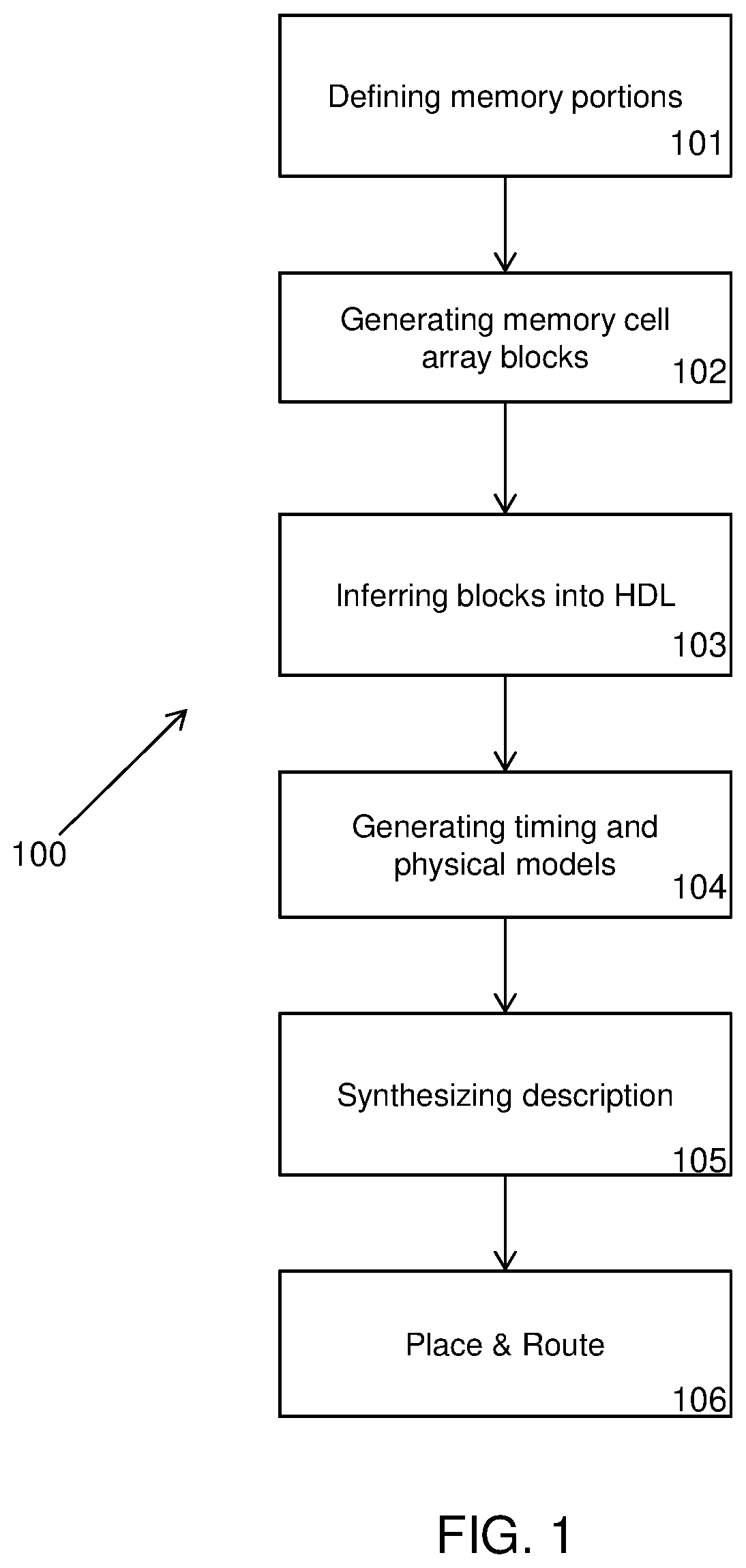
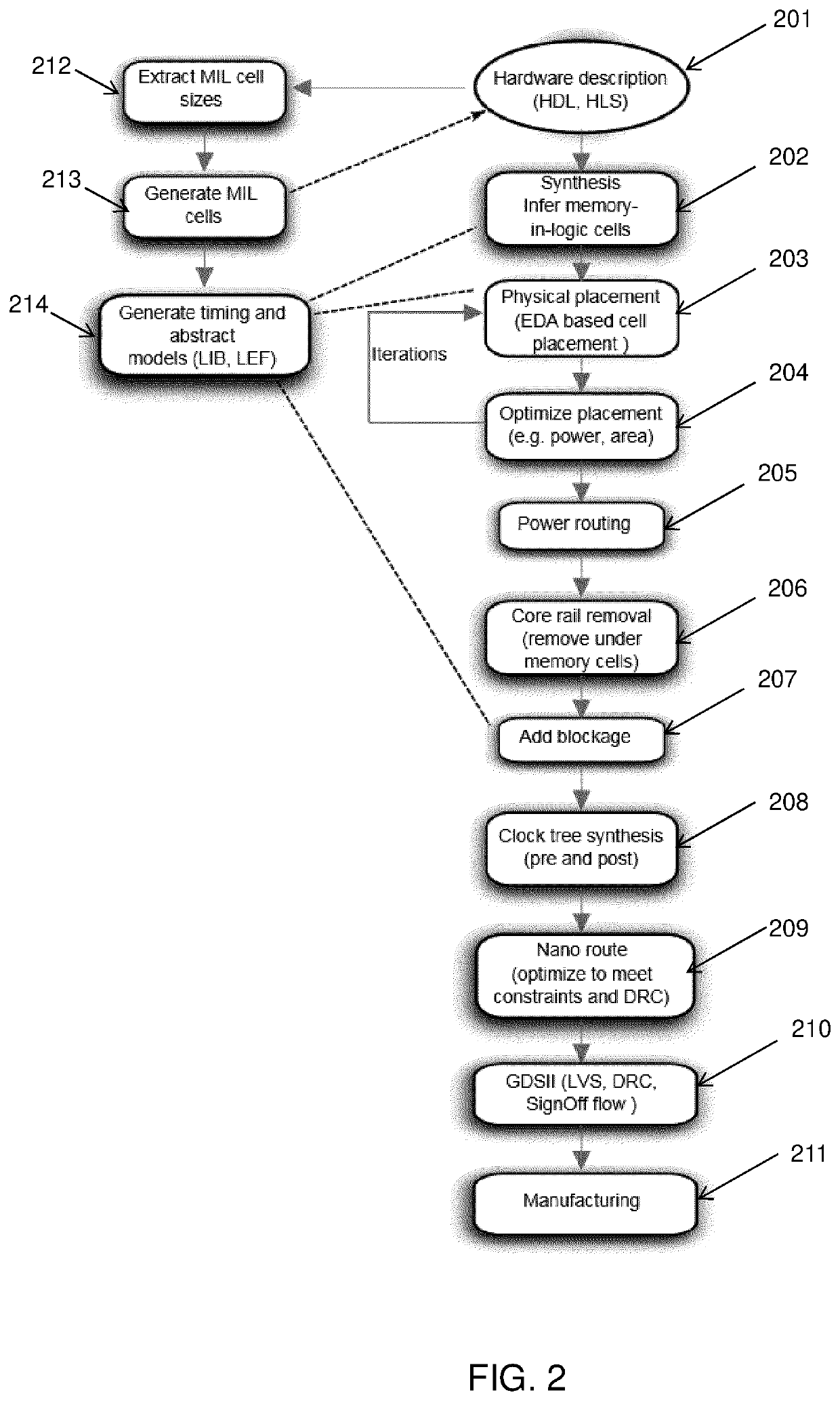
[0030]The present disclosure relates to computer-implemented method for implementing an integrated circuit comprising at least one random-access memory. The inventors have realized that by designing new memory-in-logic cells, i.e. memory cell array blocks comprising tightly packed bit cells, wherein the memory cell array blocks sizes correspond to the sizes of a number of memory portions, a more efficient integrated circuit in terms of performance and area can be achieved. By maintain the advantages of conventional memories (mainly area) and by making these blocks smaller and adapted to be integrated and placed among standard cell logic, a design can be obtained which is both area efficient and avoids, or at least improves, challenges and issues related to routing congestion. As a result, higher bandwidths and energy efficiency (pJ / access) for memory accesses can be obtained. Preferably, the method is an automated circuit design method.

[0031]In a first embodiment, the method compris...


PUM


Abstract

The present disclosure relates to a computer-implemented method for implementing an integrated circuit comprising at least one random-access memory, the method comprising the steps of: defining a plurality of memory portions of the random-access memory and obtaining sizes of the memory portions; for each memory portion, generating a memory cell array block, the memory cell array blocks corresponding to the sizes of the memory portions, wherein instances of the memory cell array blocks are inferred into a description of the integrated circuit in a hardware description language; for each memory cell array block, generating timing models and physical models; synthesizing the description of the integrated circuit in the hardware description language, including peripheral logic for the memory cell array blocks, to a schematic representation of circuit elements; placing the circuit elements, including the memory cell array blocks and the peripheral logic, on the integrated circuit and routing wires between the circuit elements taking into account the timing models and physical models of the memory cell array blocks. The disclosure further relates to an integrated circuit, comprising: a plurality of memory portions of a random-access memory, wherein each memory portion comprises a memory cell array block without, or partly without, peripheral logic; peripheral logic for each of the memory cell array block implemented as standard cells, wherein the memory cell array blocks and the peripheral logic are distributed over the circuit.

Description

[0001]The invention relates to integrated circuits (IC), random-access memories (RAM) and, more specifically to a method for implementing and / or designing an integrated circuit comprising at least one random-access memory, to a method for integration of a random-access memory in an integrated circuit and to an integrated circuit designed by said methods.BACKGROUND OF INVENTION[0002]In many modern advanced System on Chip (SoC) designs there is a need for large memory subsystems (MSS) for various requirements. Many applications require very large memories in terms of number of storage elements. At the same time there are increasing and to some extent conflicting requirements on area, access time, and power consumption.[0003]Existing RAM solutions usually try to pack bit cells in large bit cell arrays to minimize the area overhead due to RAM peripherals. This results in large RAM blocks. Although the blocks are area efficient the limited number of ports (single or dual port) can result...

Claims


Application Information

Patent Timeline
IPC IPC(8): G06F30/392G06F30/396G06F30/394G11C7/12
CPCG06F30/392G11C7/12G06F30/394G06F30/396
Inventor PRABHU, HEMANTHMOHAMMADI, BABAK
Owner XENERGIC AB
Learn More