Wafer structure

a wafer and structure technology, applied in the field of wafer structure, can solve the problems of inability to effectively reduce the number of inkjet chips required to be manufactured on the wafer structure within a limited area of less than 6 inches, and the price of inkjet printers has dropped very fast in the highly competitive inkjet printing market, so as to achieve the effect of reducing the manufacturing cost of inkjet chips, reducing the manufacturing cost, and improving the resolution

Active Publication Date: 2022-05-26
MICROJET TECH
View PDF7 Cites 0 Cited by
  • Summary
  • Abstract
  • Description
  • Claims
  • Application Information

AI Technical Summary

Benefits of technology

[0007]An object of the present disclosure is to provide a wafer structure including a chip substrate and a plurality of inkjet chips. The chip substrate is fabricated by a semiconductor process on a wafer of at least 12 inches or more, so that more required inkjet chips can be arranged on the chip substrate. Furthermore, a first inkjet chip and a second inkjet chip having different sizes of printing swath can be directly generated in the same inkjet chip semiconductor process, and a printing inkjet design for higher resolution and higher performance can be arranged thereon and diced into the first inkjet chip and the second inkjet chip used in inkjet printing, so as to achieve the object of lower manufacturing cost of the inkjet chips and the pursuit of the printing quality for higher resolution and higher printing speed.

Problems solved by technology

In addition, as the inkjet chip is pursuing the printing quality requirements of higher resolution and higher printing speed, the price of the inkjet printer has dropped very fast in the highly competitive inkjet printing market.
Therefore, the number of inkjet chips required to be manufactured on a wafer structure within a limited area of less than 6 inches become quite limited, and the manufacturing cost also cannot be effectively reduced.
Furthermore, if the inkjet chip having the printing swath more than 1 inch and / or the printing swath of one A4 page width (8.3 inches) are / is obtained with the printing quality of higher resolution and higher printing speed in the wafer structure of less than 6 inches, the number of required inkjet chips produced on the wafer structure within the limited area less than 6 inches is quite limited, and the number of the obtained inkjet chips is even lesser.
This will result in wasted remaining blank area on the wafer structure within the limited area of less than 6 inches, which occupy more than 20% of the entire area of the wafer structure, and it is quite wasteful.
Furthermore, the manufacturing cost cannot be effectively reduced.

Method used


Image

  • Wafer structure
  • Wafer structure
  • Wafer structure

Examples


Embodiment Construction

[0019]The present disclosure will now be described more specifically with reference to the following embodiments. It is to be noted that the following descriptions of preferred embodiments of this invention are presented herein for purpose of illustration and description only. It is not intended to be exhaustive or to be limited to the precise form disclosed.

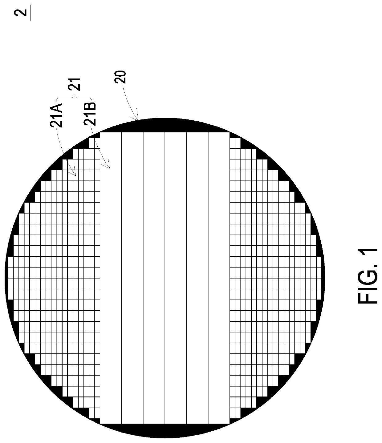
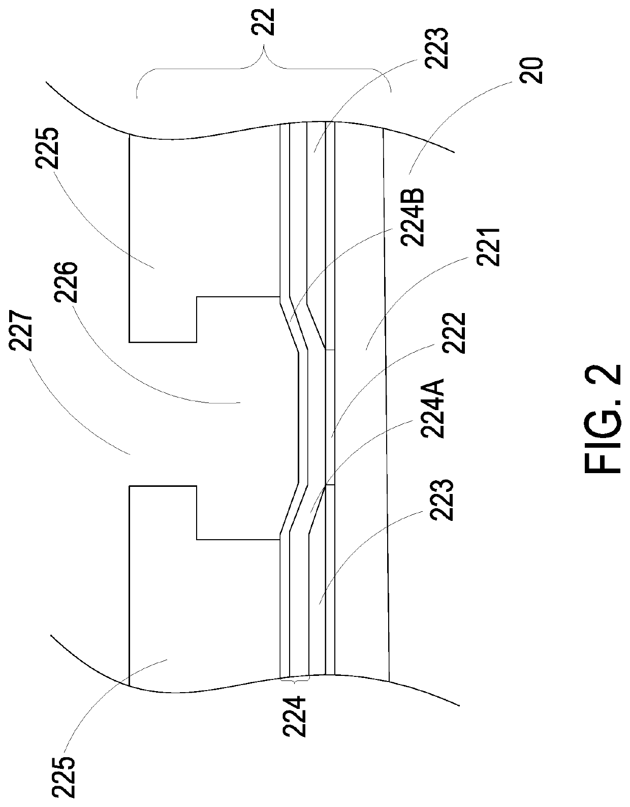
[0020]Please refer to FIG. 1. The present disclosure provides a wafer structure 2. The wafer structure 2 includes a chip substrate 20 and a plurality of inkjet chips 21. Preferably but not exclusively, the chip substrate 20 is a silicon substrate and fabricated by a semiconductor process on a wafer of at least 12 inches. In an embodiment, the chip substrate 20 is fabricated by the semiconductor process on a 12-inch wafer. In another embodiment, the chip substrate 20 is fabricated by the semiconductor process on a 16-inch wafer, but not limited thereto.

[0021]In the embodiment, the plurality of inkjet chips 21 include at least one...


PUM

PropertyMeasurementUnit
diameteraaaaaaaaaa
diameteraaaaaaaaaa
widthaaaaaaaaaa

Abstract

A wafer structure including a chip substrate and plural inkjet chips is disclosed. The chip substrate is a silicon substrate fabricated by a semiconductor process on a wafer of at least 12 inches. The inkjet chips are formed on the chip substrate by the semiconductor process and diced into the first inkjet chip and the second inkjet chip. Each of the first inkjet chip and the second inkjet chip includes plural ink-drop generators. Each of the ink-drop generators includes a nozzle. A diameter of the nozzle is in a range between 0.5 micrometers and 10 micrometers. A volume of an inkjet drop discharged from the nozzle is in a range between 1 femtoliter and 3 picoliters. The ink-drop generators form plural longitudinal axis array groups having a pitch and form plural horizontal axis array groups having a central stepped pitch equal to 1/600 inches or less.

Description

FIELD OF THE INVENTION[0001]The present disclosure relates to a wafer structure, and more particularly to a wafer structure fabricated by a semiconductor process and applied to an inkjet chip for inkjet printingBACKGROUND OF THE INVENTION[0002]In addition to a laser printer, an inkjet printer is another model that is commonly and widely used in the currently market of the printers. The inkjet printer has the advantages of low price, easy to operate and low noise. Moreover, the inkjet printer is capable of printing on various printing media, such as paper and photo paper. The printing quality of an inkjet printer mainly depends on the design factors of an ink cartridge. In particular, the design factor of an inkjet chip releasing ink droplets to the printing medium is regarded as an important consideration in the design factors of the ink cartridge.[0003]In addition, as the inkjet chip is pursuing the printing quality requirements of higher resolution and higher printing speed, the p...

Claims


Application Information

Patent Timeline
Patent Type & Authority Applications(United States)
IPC IPC(8): B41J2/14B41J2/145
CPCB41J2/14112B41J2/14145B41J2/14072B41J2/145B41J2/14B41J2/14129B41J2/15B41J2002/14459B41J2202/11B41J2202/13B41J2/14024
Inventor MOU, HAO-JANCHANG, YING-LUNTAI, HSIEN-CHUNGHAN, YUNG-LUNGHUANG, CHI-FENGTSAI, CHANG-YEN
Owner MICROJET TECH
Why Eureka
Try Eureka