Display panel, manufacturing method thereof, and display device

a technology of display panel and manufacturing method, applied in the field of display panel, can solve the problems of reducing affecting the electrical conductivity of cu electrodes, and the process temperature window of bce-tft backplate technology is relatively low, so as to reduce the manufacturing process of display panel and reduce manufacturing costs. , the effect of poor bonding for

Active Publication Date: 2022-06-16
SHENZHEN CHINA STAR OPTOELECTRONICS SEMICON DISPLAY TECH CO LTD
View PDF0 Cites 0 Cited by
  • Summary
  • Abstract
  • Description
  • Claims
  • Application Information

AI Technical Summary

Benefits of technology

[0004]The present application provides a display panel, a manufacturing method thereof, and a display device, which can effectively solve problems of a poor bonding force between MoTiNi (MTD) and a soldering material, reduce manufacturing processes of the display panel, and reduce manufacturing costs.
[0041]The present application adopts at least one of the molybdenum / copper stackup, the molybdenum-titanium alloy / copper stackup, or the titanium-molybdenum-nickel alloy / copper stackup to form the solder pad for bonding, which can effectively solve the problem of the poor bonding force between MTD and the soldering material in the prior art. Meanwhile, the bonding lead is made of titanium-molybdenum-nickel alloy / copper / titanium-molybdenum-nickel alloy stackup, which can reduce manufacturing processes of the display panel and reduce manufacturing costs.

Problems solved by technology

However, a process temperature window of the BCE-TFT backplate technology is relatively low, and an increase of the PV film forming temperature easily causes the Cu electrodes to oxidize and affect electrical conductivity.
In addition, heat treatment temperature required for metal oxide semiconductors varies with a material composition, and some oxides require a high-temperature manufacturing process, and this technology cannot be better compatible.
However, a solder paste bonding force required for bonding this alloy and an LED is poor, which affects a bonding effect.

Method used


Image

  • Display panel, manufacturing method thereof, and display device
  • Display panel, manufacturing method thereof, and display device
  • Display panel, manufacturing method thereof, and display device

Examples


first embodiment

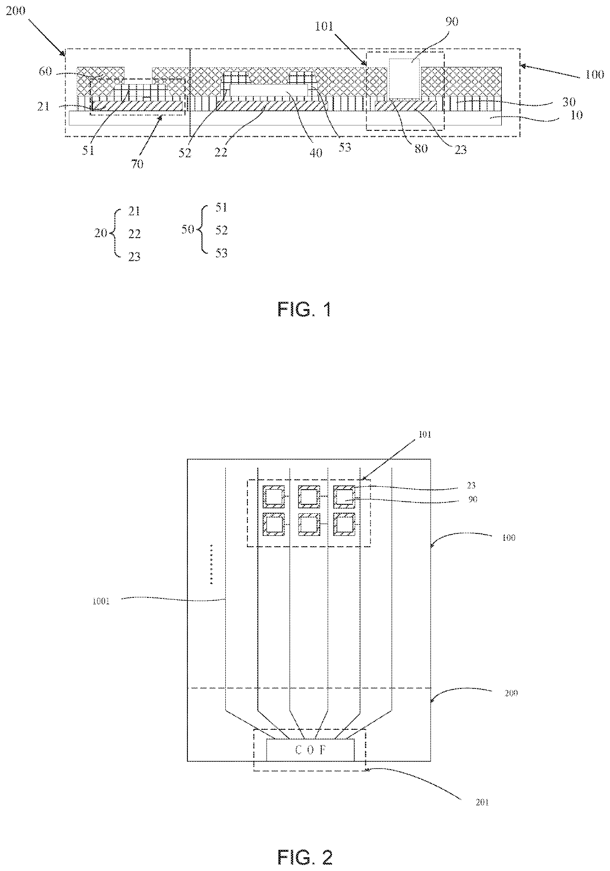
[0047]Please refer to FIG. 1, which is a structural schematic diagram of a display panel provided by an embodiment of the present application.

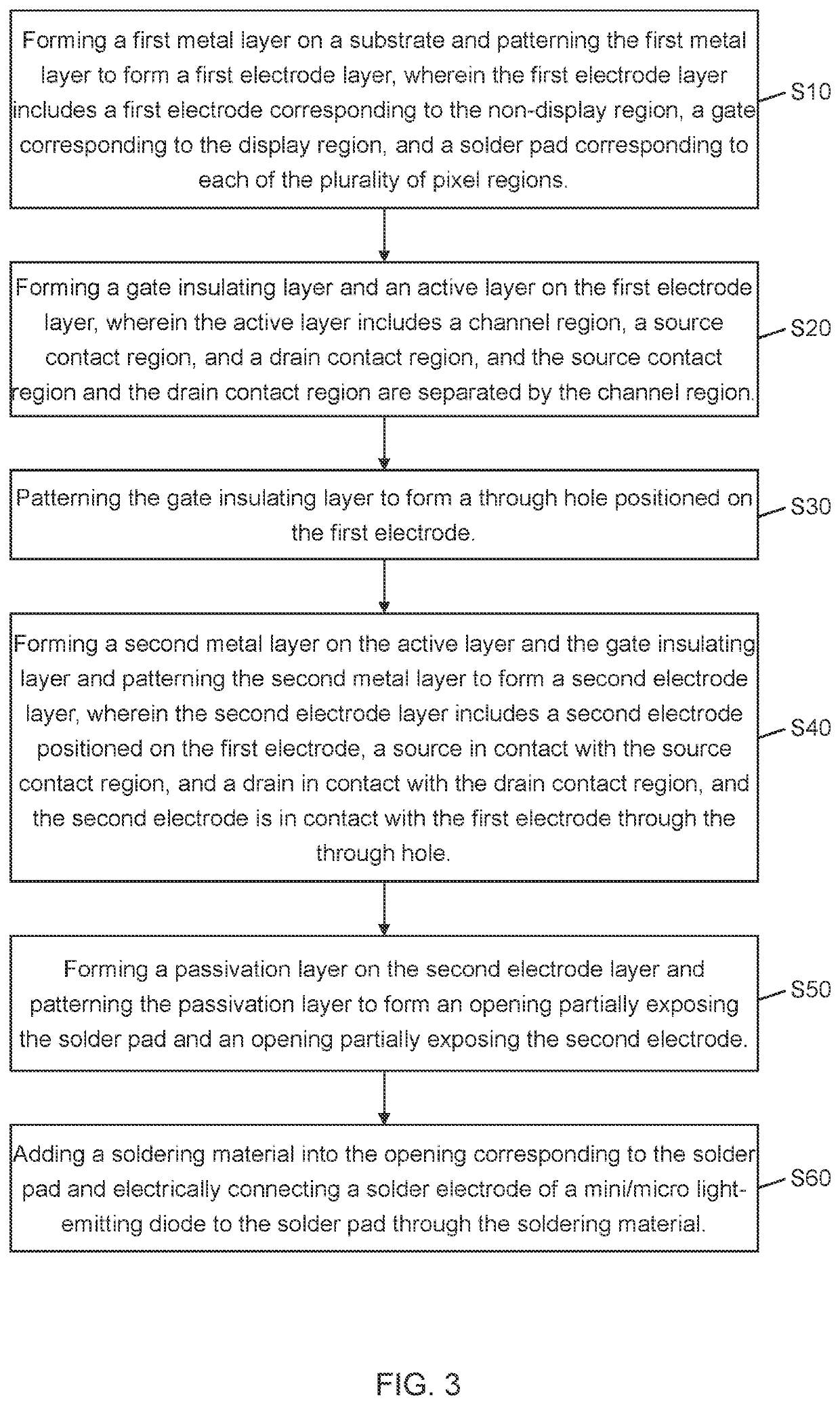
[0048]In the present application, the display panel includes a display region 100 and a non-display region 200 surrounding the display region. The display region 100 includes a plurality of pixel regions 101.

[0049]The display panel includes a substrate 10, a first electrode layer 20 disposed on the substrate 10, a first insulating layer 30 disposed on the first electrode layer 20, an active layer 40 disposed on the first insulating layer 30, a second electrode layer 50 disposed on the active layer 40, and a second insulating layer 60 disposed on the second electrode layer 50.

[0050]In this embodiment, the substrate 10 is a PI substrate, which is mainly polyimide. PI material can effectively increase light transmittance.

[0051]In this embodiment, the first electrode layer 20 includes a first electrode 21, a gate 22, and a solder pad 23, which are...

second embodiment

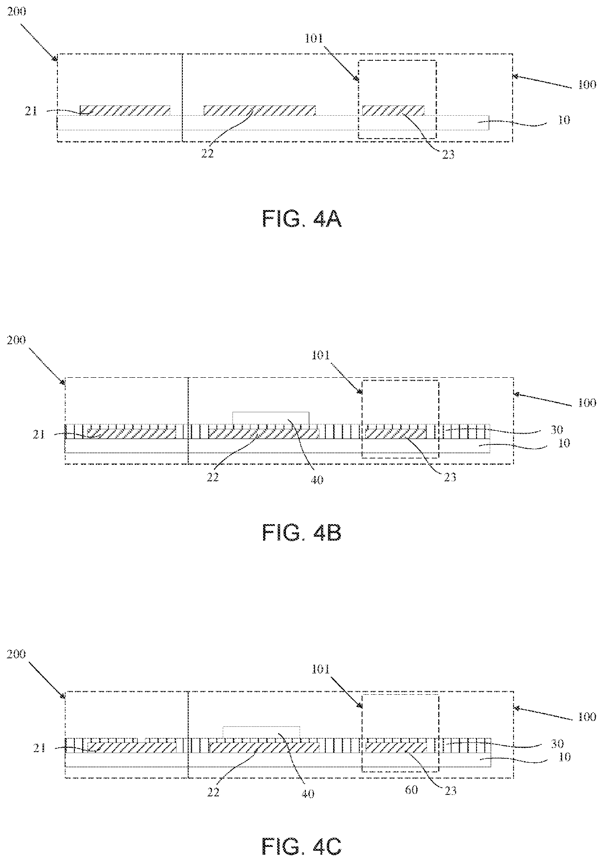
[0082]Please refer to FIG. 3, which is a flowchart of a manufacturing method of a display panel provided by an embodiment of the present application.

[0083]In this embodiment, the display panel includes a display region 100 and a non-display region 200 surrounding the display region 100. The display region 100 includes a plurality of pixel regions 101.

[0084]The manufacturing method includes the following steps.

[0085]Step S10: providing a substrate 10, forming a first metal layer on the substrate 10, and patterning the first metal layer to form a first electrode layer 20, wherein the first electrode layer 20 includes a first electrode 21 corresponding to the non-display region 200, a gate 22 corresponding to the display region 100, and a solder pad 23 corresponding to each of the plurality of pixel regions 101, as shown in FIG. 4A.

[0086]In this embodiment, the substrate 10 is a PI substrate, which is mainly polyimide. PI material can effectively increase light transmittance.

[0087]In t...

third embodiment

[0103]The present application further provides a display device. The display device includes the display panel in the first embodiment.

[0104]The display panel has been described in detail in the first embodiment, which is not repeated herein.

[0105]In summary, the present application provides the display panel, the manufacturing method thereof, and the display device. The display panel includes the display region and the non-display region surrounding the display region. The display region includes the plurality of pixel regions. The display panel includes the substrate, and the solder pad and the signal line disposed on the substrate. The solder pad corresponds to each of the plurality of pixel regions and is electrically connected to the signal line. Material of the solder pad includes at least one of the molybdenum / copper stackup, the molybdenum-titanium alloy / copper stackup, or the titanium-molybdenum-nickel alloy / copper stackup. The solder electrode of the mini / micro light-emitt...


PUM

PropertyMeasurementUnit
insulatingaaaaaaaaaa
brightnessaaaaaaaaaa
electrical conductivityaaaaaaaaaa

Abstract

The present application provides a display panel, a manufacturing method thereof, and a display device. The present application adopts a molybdenum / copper stackup to form a solder pad for bonding, which can effectively solve a problem of a poor bonding force between MTD and a soldering material in the prior art. Meanwhile, a bonding lead is made of titanium-molybdenum-nickel alloy / copper / titanium-molybdenum-nickel alloy stackup, which can reduce manufacturing processes of the display panel and reduce manufacturing costs.

Description

FIELD OF INVENTION[0001]The present application is related to the field of display technology, and specifically, to a display panel, a manufacturing method thereof, and a display device.BACKGROUND OF INVENTION[0002]Mini / micro light-emitting diode (MLED) display technology has entered an accelerated development stage in past two years and can be used in small-and-medium-sized and high-value-added display applications. Compared with organic light-emitting diode (OLED) displays, MLED displays can show better performance in terms of cost, contrast, high brightness, and thin-and-light appearance.[0003]In the MLED display technology, backplate technology is a key technology, and optimizing backplate technology is essential for the MLED display technology. A conventional BCE-TFT backplate technology uses 6-mask technology, wherein M2 uses Mo / Cu metal as an LED bonding pad and uses ITO as a COF bonding protective layer to prevent Cu electrodes from oxidation. However, a process temperature ...

Claims


Application Information

Patent Timeline
Patent Type & Authority Applications(United States)
IPC IPC(8): H01L33/62H01L33/40H01L25/075
CPCH01L33/62H01L33/40H01L2933/0066H01L2933/0016H01L25/0753H01L27/156H01L25/167
Inventor MEI, XUERULU, MACAI
Owner SHENZHEN CHINA STAR OPTOELECTRONICS SEMICON DISPLAY TECH CO LTD
Why Eureka
Try Eureka