Quantum bit cell and quantum bit integrated circuit

Pending Publication Date: 2022-07-14
NAT INST OF ADVANCED IND SCI & TECH
View PDF0 Cites 0 Cited by
  • Summary
  • Abstract
  • Description
  • Claims
  • Application Information

AI Technical Summary

Benefits of technology

The present invention provides a solution to problems in conventional technology by providing a quantum bit cell and a quantum bit integrated circuit that have an easy-to-integrate structure.

Problems solved by technology

However, since the high-frequency transmission line is large in size unlike power supply wiring and the shape for transmitting the microwave is constrained, it tends to increase the area and is difficult to manufacture, which become factors that hinder the construction of a multi-bit integrated circuit in which many solid-state element quantum bits mentioned above are arranged.
Further, the high-frequency transmission line easily generates a so-called crosstalk to affect any other solid-state element quantum bit different from the target solid-state element quantum bit, which becomes a factor that hinders selective operation to each individual solid-state element quantum bit.
However, since the micromagnet has a size of a few tens of gm order, much bigger than the size of the solid-state element quantum bit, which becomes rather a hindrance to integration of solid-state element quantum bits.

Method used


Image

  • Quantum bit cell and quantum bit integrated circuit
  • Quantum bit cell and quantum bit integrated circuit
  • Quantum bit cell and quantum bit integrated circuit

Examples


first embodiment

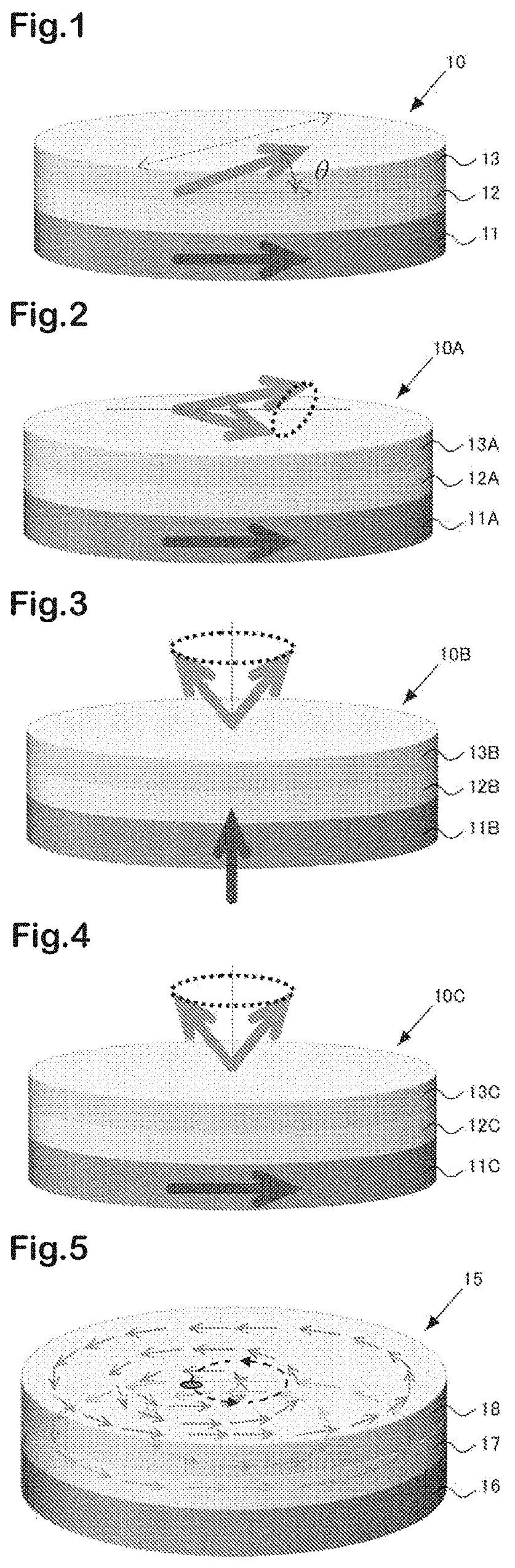
[0157]Next, embodiments of the quantum bit cell according to the present invention will be described with reference to the accompanying drawings.

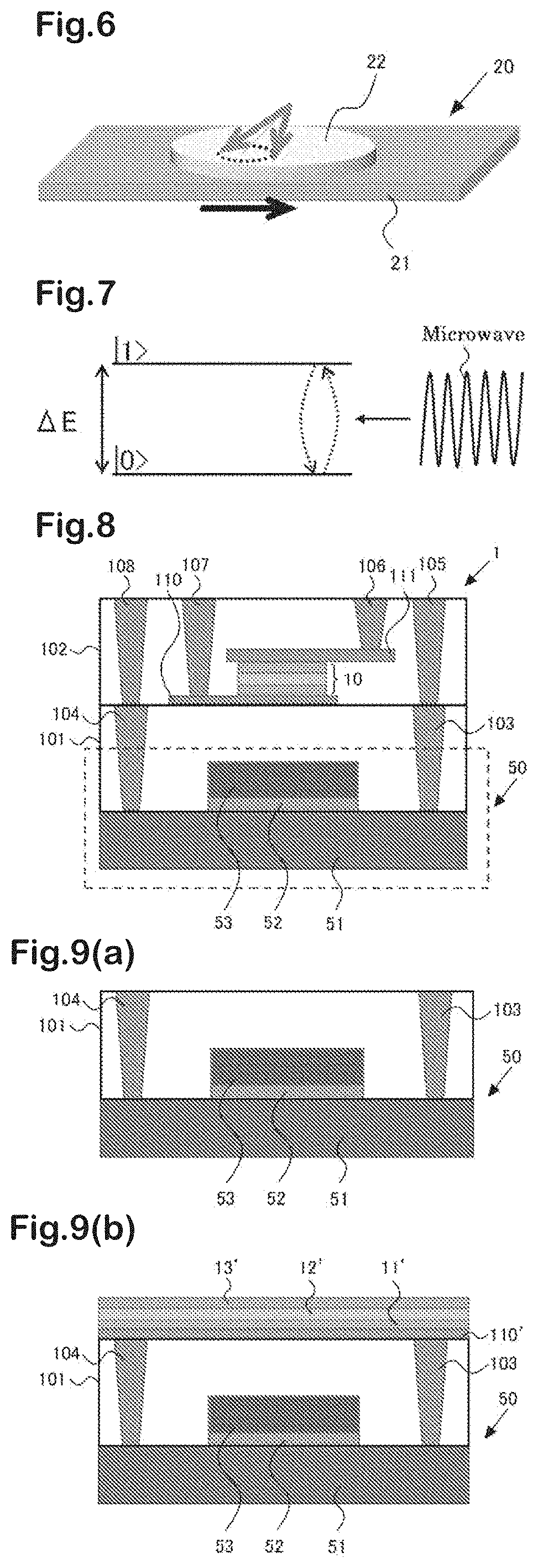
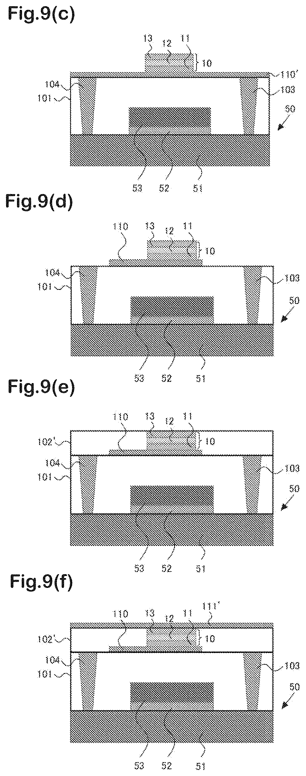
[0158]First, a quantum bit cell according to a first embodiment will be described with reference to FIG. 8. Note that FIG. 8 is a sectional view for describing an overview of the quantum bit cell according to the first embodiment.

[0159]As illustrated in FIG. 8, a quantum bit cell 1 according to the first embodiment has the spin valve-type element 10 (see FIG. 1) as the spin torque oscillator, and a semiconductor quantum bit element 50 as the solid-state element quantum bit.

[0160]The semiconductor quantum bit element 50 has a transistor structure in which a gate electrode 53 is placed above a channel region of a semiconductor-containing layer 51 through an insulating oxide film 52, where the channel region is made of a semiconductor material and formed between the source section and the drain section.

[0161]The semiconductor-containing layer ...

second embodiment

[0186]Next, a quantum bit cell according to a second embodiment will be described with reference to FIG. 10. Note that FIG. 10 is a sectional view for describing an overview of the quantum bit cell according to the second embodiment.

[0187]As illustrated in FIG. 10, a quantum bit cell 1′ according to the second embodiment has the spin orbit torque-excited element 20 (see FIG. 6) as the spin torque oscillator and the semiconductor quantum bit element 50 as the solid-state element quantum bit, which is different from the quantum bit cell 1 according to the first embodiment in that the spin orbit torque-excited element 20 is arranged as the spin torque oscillator instead of the spin valve-type element 10. Since the other components are the same as those in the quantum bit cell 1 according to the first embodiment, the same reference numerals are illustrated to omit redundant description.

[0188]Here, the size of the spin orbit torque-excited element 20 can be set to have a maximum diameter...

examples

[0209]In order to clarify the respective characteristics of the solid-state element quantum bit and the spin torque oscillator that constitute the quantum bit cell of the present invention, the solid-state element quantum bit and the spin torque oscillator were manufactured individually, and the characteristics were measured. The details will be described below.

[0210]

[0211]The semiconductor quantum bit element having the transistor structure was manufactured as below as the solid-state element quantum bit in a working example.

[0212]First, an SOI wafer in which an SiO2 insulation layer (BOX layer) with a thickness of 145 nm and the semiconductor layer (the semiconductor-containing layer) made of Si and doped with about 1×101s cm−3 of p-type impurities having a thickness of 50 nm are formed in this order on a handling Si layer was prepared.

[0213]Next, a protective oxide film is formed with a thickness of 5 nm on the semiconductor layer of this SOI wafer.

[0214]Next, a first resist laye...


PUM


Abstract

The present invention addresses the problem of providing a quantum bit cell and a quantum bit integrated circuit having an easy-to-integrate structure. The quantum bit cell of the present invention including a spin torque oscillator capable of emitting a microwave with a propagation distance of 1 μm or less and having a maximum diameter of 1 μm or less, and a solid-state element quantum bit arranged near the spin torque oscillator at an interval of the propagation distance or less, where a quantum two-level system is controlled by the microwave.

Description

TECHNICAL FIELD[0001]The present invention relates to a quantum bit cell in which a solid-state element quantum bit and a spin torque oscillator are arranged, and a quantum bit integrated circuit in which multiple quantum bit cells are arranged.BACKGROUND ART[0002]Research on a solid-state element quantum bit with a quantum two-level system controlled by a microwave is underway.[0003]The solid-state element quantum bit generally requires a cryogenic operating environment of 100 mK or less, and is arranged inside a temperature control device for cryogenic use such as a cryostat.[0004]A microwave generator placed outside of the temperature control device as a supply source introduces the microwave from outside of the temperature control device into the temperature control device to supply the microwave to the solid-state element quantum bit as a target in order to control the state of the quantum bit.[0005]For example, after the microwave is introduced into the temperature control dev...

Claims


Application Information

Patent Timeline
IPC IPC(8): G06N10/40H01L43/08H01L43/02
CPCG06N10/40H01L43/02H01L43/08H01L29/82H01L29/06H10N50/10H10N50/80
Inventor KUBOTA, HITOSHITAMARU, SHINGOFUKUSHIMA, AKIOMORI, TAKAHIROMATSUKAWA, TAKASHI
Owner NAT INST OF ADVANCED IND SCI & TECH
Why Eureka
Try Eureka