Circuit board and manufacturing method thereof and electronic device

a technology of circuit boards and manufacturing methods, applied in the field of circuit boards, can solve problems such as affecting high-frequency signal integrity and noise interference cannot be reduced

Pending Publication Date: 2022-07-21
UNIMICRON TECH CORP
View PDF0 Cites 2 Cited by
  • Summary
  • Abstract
  • Description
  • Claims
  • Application Information

AI Technical Summary

Problems solved by technology

Therefore, there may be impedance mismatch and a gap of electromagnetic interference (EMI) shielding at the two ends of the coaxial via, affecting high-frequency signal integrity.
In add...

Method used


Image

  • Circuit board and manufacturing method thereof and electronic device
  • Circuit board and manufacturing method thereof and electronic device
  • Circuit board and manufacturing method thereof and electronic device

Examples


Embodiment Construction

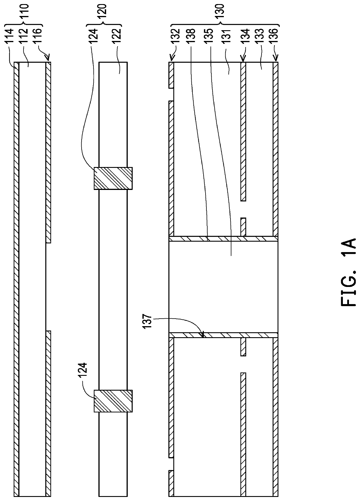
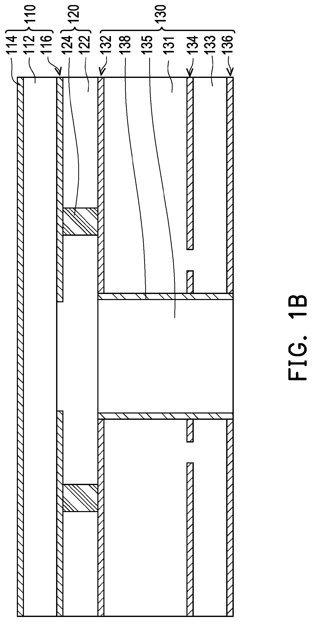
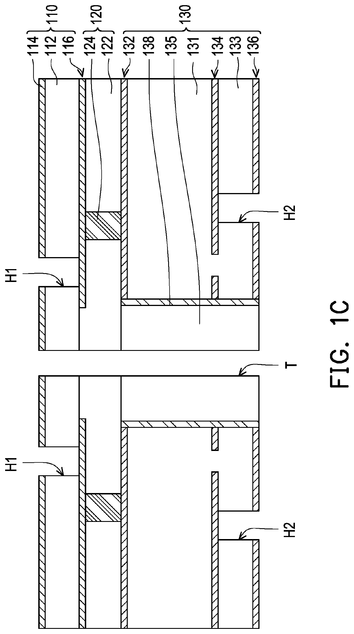
[0030]FIG. 1A to FIG. 1E are schematic cross-sectional diagrams of a manufacturing method of a circuit board according to an embodiment of the disclosure. FIG. 1F is a top-view of a circuit board of FIG. 1E. In the manufacturing method of the circuit board according to the embodiment, referring to FIG. 1A, a first substrate 110, a second substrate 120, a third substrate 130 are provided.

[0031]Specifically, in the embodiment, the first substrate 110 includes a core layer 112, a first conductive layer 114, and a first circuit layer 116. The first conductive layer 114 and the first circuit layer 116 are respectively disposed on two opposite sides of the core layer 112. The first conductive layer 114 is not patterned and completely covers a side surface of the core layer 112, and the first circuit layer 116 is exposed out of a portion of another side surface of the core layer 112. Here, a material of the core layer 112 is, for example, a dielectric material. A dielectric constant (Dk) o...


PUM


Abstract

A circuit board includes a first substrate, a second substrate, a third substrate, a plurality of conductive structures and a conductive via structure. The second substrate is disposed between the first substrate and the third substrate. The third substrate has an opening and includes a first dielectric layer, a second dielectric layer, and a third dielectric layer. The opening penetrates the first dielectric layer and the second dielectric layer, and the third dielectric layer fully fills the opening. The conductive via structure penetrates the first substrate, the second substrate, the third dielectric layer of the third substrate, and is electrically connected to the first substrate and the third substrate to define a signal path. The first substrate, the second substrate, and the third substrate are electrically connected through the conductive structures to define a ground path, and the ground path surrounds the signal path.

Description

CROSS-REFERENCE TO RELATED APPLICATION[0001]This application is a continuation-in-part application of and claims the priority benefit of U.S. application Ser. No. 17 / 498,757, filed on Oct. 12, 2021, now pending. The prior U.S. application Ser. No. 17 / 498,757 claims the priority benefits of U.S. provisional application Ser. No. 63 / 139,795, filed on Jan. 21, 2021, U.S. provisional application Ser. No. 63 / 235,105, filed on Aug. 19, 2021, and Taiwan application serial no. 110134179, filed on Sep. 14, 2021. The entirety of each of the above-mentioned patent applications is hereby incorporated by reference herein and made a part of this specification.BACKGROUNDTechnical Field[0002]The disclosure relates to a substrate structure and a manufacturing method thereof, and in particular, to a circuit board and a manufacturing method thereof and an electronic device adopting the circuit board.Description of Related Art[0003]In a conventional circuit board, a design of a coaxial via requires one ...

Claims


Application Information

Patent Timeline
IPC IPC(8): H05K1/02H05K1/11H05K3/42H05K3/00
CPCH05K1/0231H05K1/116H05K1/0298H05K3/429H05K3/421H05K3/0094H05K2203/1461H05K2201/0723H05K2201/09509H05K2201/0959H05K2201/09645H05K2203/0502H05K2201/0195H05K2203/061H05K2201/09618H05K1/113H05K1/115H05K1/0219H01L23/49827H01L23/49822
Inventor HUANG, JUN-RUILU, CHIH-CHIANGLIN, YI-PINCHEN, CHING-SHENG
Owner UNIMICRON TECH CORP
Why Eureka
Try Eureka