

Circuit board and manufacturing method thereof and electronic device
a technology of circuit boards and manufacturing methods, applied in the field of circuit boards, can solve problems such as affecting the integrity of high-frequency signals and the inability to reduce noise interferen
- Summary
- Abstract
- Description
- Claims
- Application Information
AI Technical Summary
Benefits of technology
Problems solved by technology
Method used
Image

Examples
Embodiment Construction
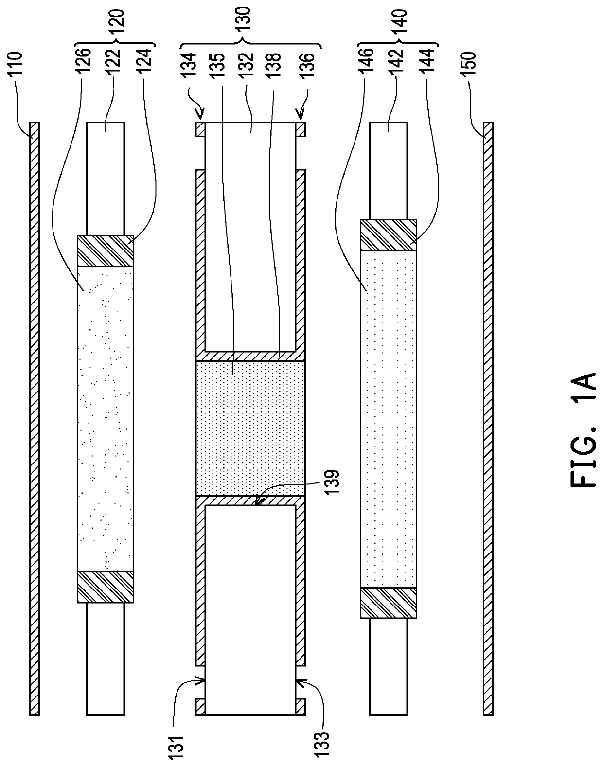
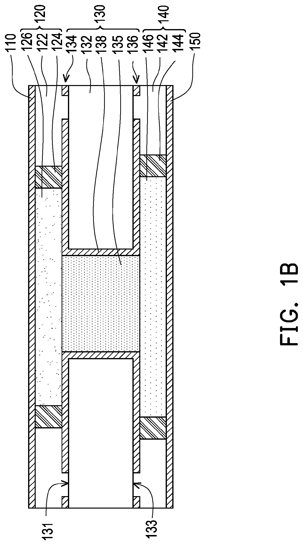
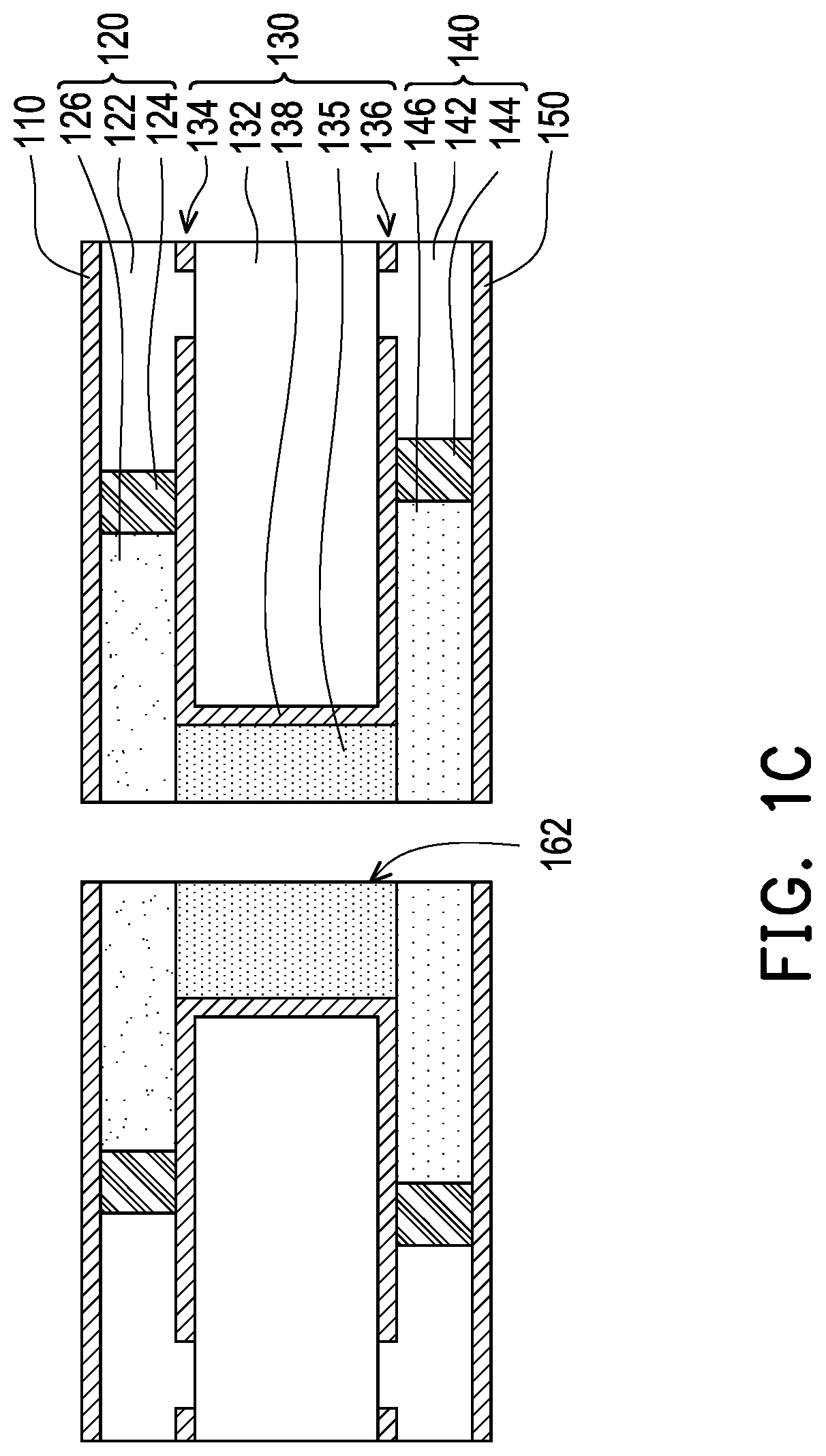
[0062]FIG. 1A to FIG. 1E are schematic cross-sectional diagrams of a manufacturing method of a circuit board according to an embodiment of the disclosure. FIG. 1F is a top-view of a circuit board of FIG. 1E. In the manufacturing method of the circuit board according to the embodiment, referring to FIG. 1A, a first metal layer 110, a first base material 120, a second base material 130, a third base material 140, and a second metal layer 150 are provided. The first base material 120 includes a first substrate 122, first conductive pillars 124, and a first dielectric material 126. The first dielectric material 126 and the first conductive pillars 124 penetrate the first substrate 122, and the first conductive pillars 124 are located between the first substrate 122 and the first dielectric material 126. The first conductive pillars 124 surround the first dielectric material 126. Providing the first base material 120 includes the following. First, the first substrate 122 is provided. The...
PUM
| Property | Measurement | Unit |
|---|---|---|
| dielectric dissipation factor | aaaaa | aaaaa |
| dielectric constant | aaaaa | aaaaa |
| dielectric dissipation factor | aaaaa | aaaaa |
Abstract
Description
Claims
Application Information