

Display apparatus
a technology of display apparatus and display surface, which is applied in the direction of identification means, instruments, semiconductor devices, etc., can solve the problems of poor light extraction efficiency of light-emitting diodes, poor color uniformity, and more susceptible damage of light-emitting diodes
- Summary
- Abstract
- Description
- Claims
- Application Information
AI Technical Summary
Benefits of technology
Problems solved by technology
Method used
Image

Examples
first embodiment
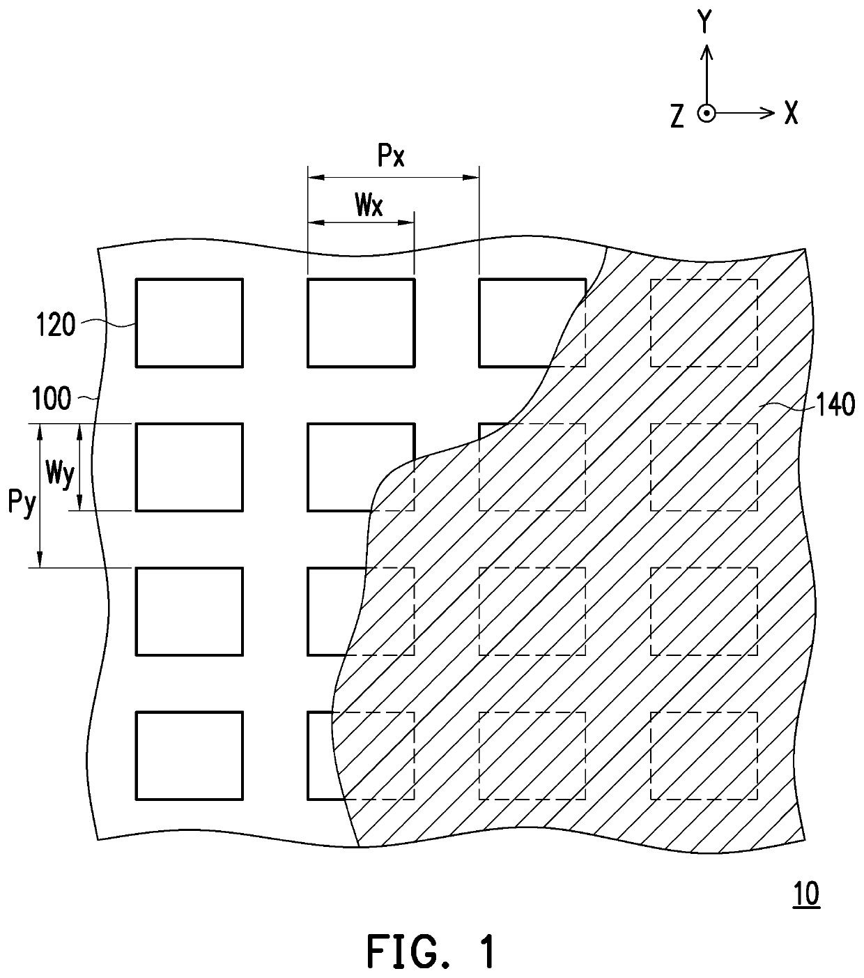
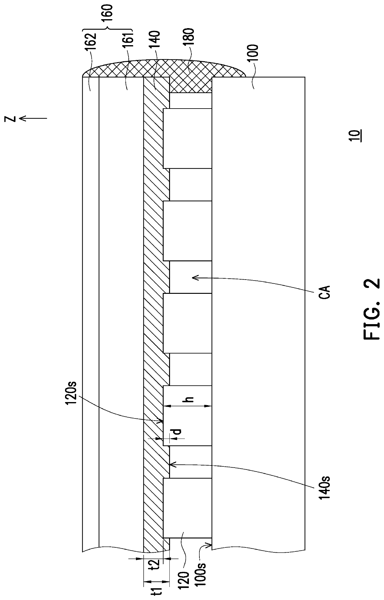
[0031]FIG. 1 is a schematic top view of a display apparatus according to the disclosure. FIG. 2 is a schematic cross-sectional view of the display apparatus of FIG. 1. Referring to FIG. 1 and FIG. 2, a display apparatus 10 includes a circuit substrate 100, a plurality of light-emitting elements 120, an adhesive layer 140, and an optical film 160. The light-emitting elements 120 are dispersedly disposed on a substrate surface 100s of the circuit substrate 100 and are electrically bonded to the circuit substrate 100. For example, the light-emitting elements 120 may be disposed in multiple columns and multiple rows along the direction X and the direction Y, respectively. The direction X is perpendicular to the direction Y. That is, the light-emitting elements 120 can be disposed in an array on the circuit substrate 100, but the disclosure is not limited thereto.
[0032]In the embodiment, the circuit substrate 100 is a printed circuit substrate (PCB), for example, but the disclosure is no...
second embodiment
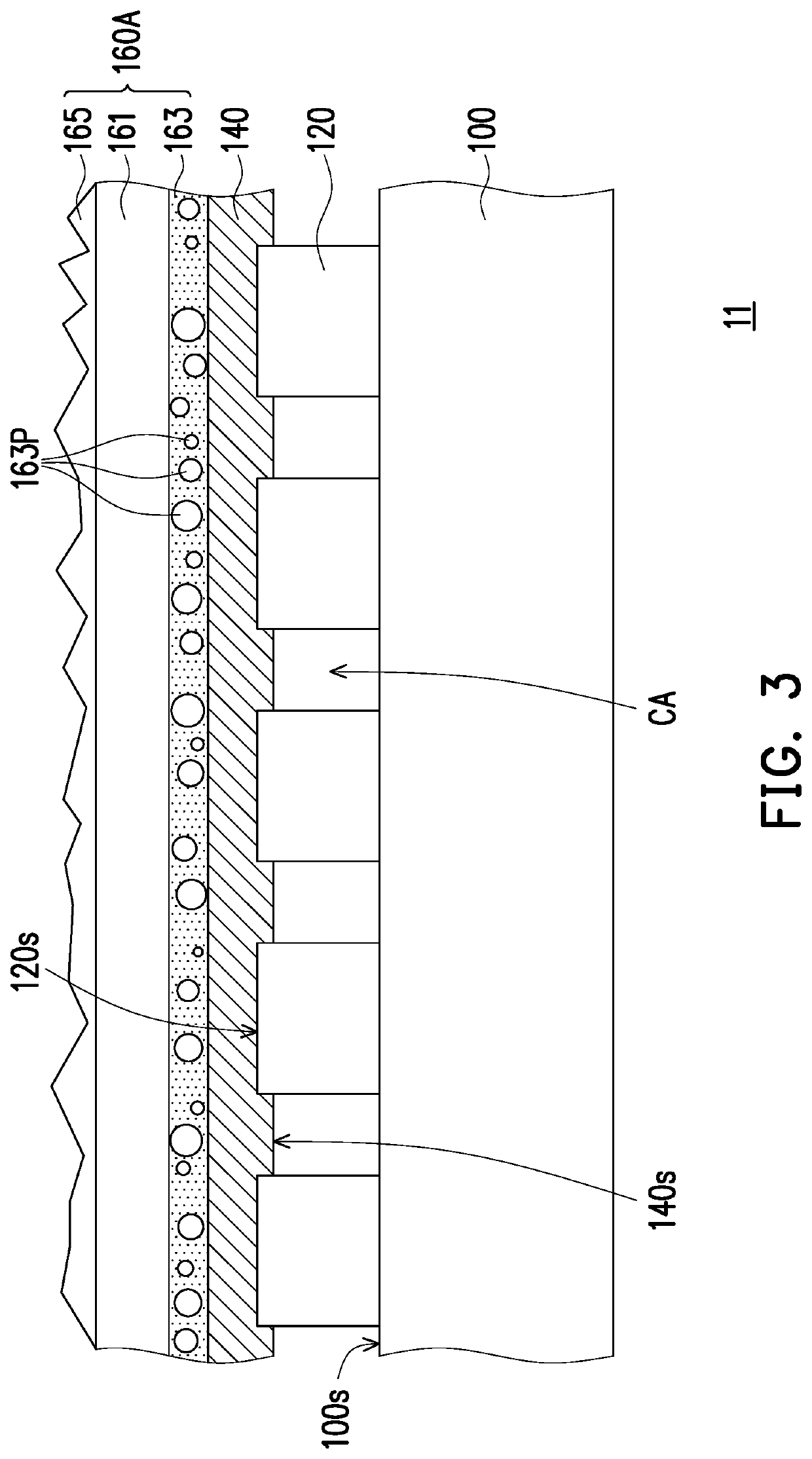
[0044]FIG. 3 is a schematic cross-sectional view of a display apparatus according to the disclosure. Referring to FIG. 3, the main difference between a display apparatus 11 of the embodiment and the display apparatus 10 of FIG. 2 is that the composition of the optical film is different. Specifically, an optical film 160A of the display apparatus 11 has an overlapped structure of the polarizing layer 161, an anti-glare adhesive layer 163, and a surface treatment layer 165. The anti-glare adhesive layer 163 is disposed between the polarizing layer 161 and the adhesive layer 140. The polarizing layer 161 is disposed between the anti-glare adhesive layer 163 and the surface treatment layer 165. In the embodiment, the anti-glare adhesive layer 163 may include a glue material and a plurality of scattering particles 163P doped in the glue material. For example, the glue material is an optical pressure sensitive adhesive, and the material of the scattering particles 163P includes silicone r...
fifth embodiment
[0048]FIG. 6 is a schematic cross-sectional view of a display apparatus according to the disclosure. Referring to FIG. 6, the difference between a display apparatus 14 of the embodiment and the display apparatus 10 of FIG. 2 is that the composition of the optical film is different. Specifically, an optical film 160D of the display apparatus 14 is an overlapped structure of the polarizing layer 161, a refracting layer 164, and a surface treatment layer 166, and the refracting layer 164 is disposed between the surface treatment layer 166 and the polarizing layer 161.
[0049]For example, in the embodiment, the refracting layer 164 may have a plurality of optical microstructures 164MS. For example, the optical microstructures 164MS are a plurality of microprisms and adapted for deflecting light LB from the light-emitting element 120 to a specific light emitting range, and the light concentration of the display apparatus 14 is increased. In the embodiment, the surface treatment layer 166 i...
PUM
 Abstract
Description
Claims
Application Information