Integrated waveguide polarizer

a waveguide polarizer and integrated technology, applied in the direction of optical waveguide light guides, instruments, optical light guides, etc., can solve the problem of not intended summary, and achieve the effect of broad optical bandwidth, low device loss, and high extinction ratio

Active Publication Date: 2022-08-11
ALPINE OPTOELECTRONICS INC
View PDF6 Cites 2 Cited by
  • Summary
  • Abstract
  • Description
  • Claims
  • Application Information

AI Technical Summary

Benefits of technology

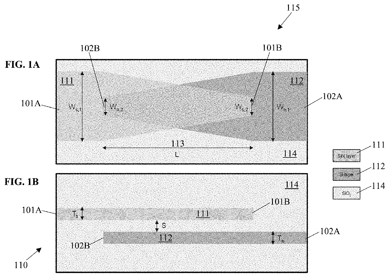
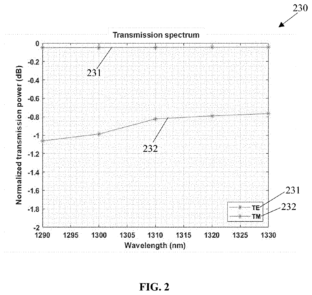
[0007]In an aspect, an integrated waveguide polarizer is provided. The integrated waveguide polarizer may comprise: a plurality of silicon layers and a plurality of silicon-nitride layers; each of the plurality of silicon layers and each of the plurality of silicon-nitride layers having a first end and an opposite second end, the first end having a selectively wide width and the second end having a selectively narrow width, such that each silicon layer and each silicon-nitride layer have tapered shapes; wherein each silicon-nitride layer is disposed above each silicon layer, such that at least a portion of each silicon-nitride layer overlaps at least a portion of each silicon layer; and a plurality of oxide layers disposed between the pluralities of silicon-nitride layers and silicon layers, each oxide layer of the plurality of oxide layers creating a separation spacing between each silicon-nitride layer and each silicon layer; wherein, when an optical signal is launched through the integrated waveguide polarizer, the optical signal is caused to transition between each silicon-nitride layer and each silicon layer via the overlapped portions of each silicon-nitride and silicon layers, the transitioning between each silicon-nitride and silicon layers inducing losses on the transverse-electric (TE) and the transverse-magnetic (TM) polarization states of the optical signal, the induced loss on the TE polarization state being lower than the induced loss on the TM polarization state. Thus, an advantage is that the SiN—Si or Si—SiN transition of the integrated waveguide polarizer may realize a high extinction ratio. Another advantage is that the SiN—Si or Si—SiN transition of the disclosed waveguide polarizer may show low device loss for the TE polarization state. An additional advantage is that the SiN—Si or Si—SiN transition of the disclosed waveguide polarizer may realize a broad optical bandwidth.
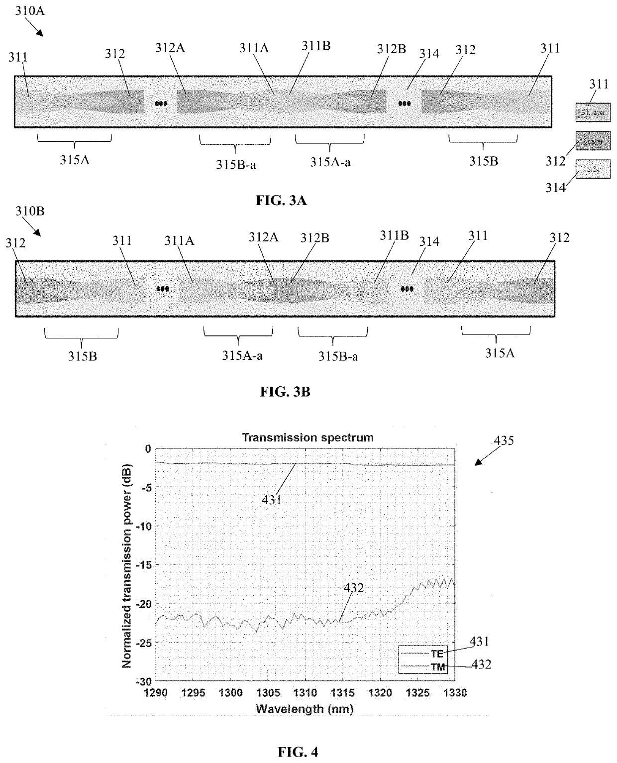
[0008]In another aspect, an integrated waveguide polarizer is provided. The integrated waveguide polarizer may comprise a plurality of cascaded layer transitions, each cascaded layer transition of the plurality of cascaded layer transitions having a silicon (Si) layer and a silicon-nitride (SiN) layer each having a first end and an opposite second end, the first end having a selectively wide width and the second end having a selectively narrow width, such that the silicon layer and the silicon-nitride layer each has a tapered shape, the silicon-nitride layer being disposed above the silicon layer, such that at least a portion of the silicon-nitride layer overlaps at least a portion of the silicon layer, such that the second ends of the silicon-nitride layer and the silicon layer are overlapped and oriented to face in opposite directions, and wherein a first and a second cascaded layer transitions of the plurality of cascaded layer transitions are coaxially aligned, such that the first ends of a first and a second silicon-nitride layers of the first and the second cascaded layer transitions, respectively, are coaxially aligned and joined, such that the second ends of a first and a second silicon layers of the first and the second cascaded layer transitions, respectively, are oriented to face each other. Thus, an advantage is that the cascaded SiN—Si and Si—SiN transitions of the integrated waveguide polarizer may realize a high extinction ratio. Another advantage is that the cascaded SiN—Si and Si—SiN transitions of the disclosed waveguide polarizer may show low device loss for the TE polarization state. An additional advantage is that the SiN—Si and Si—SiN transitions of the disclosed waveguide polarizer may realize a broad optical bandwidth.
[0009]In another aspect, a method of integrating a waveguide polarizer onto an optical waveguide of an integrated photonics chip is provided. The method may comprise the steps of: depositing a plurality of first layers each having a first end and an opposite second end onto the optical waveguide, each first end having a selectively wide width and each second end having a selectively narrow width; providing an oxide layer having a thickness atop each first layer of the plurality of first layers, the oxide layer providing a separation spacing above each first layer; and depositing a plurality of second layers each having a first end and an opposite second end atop each of the oxide layers, such that at least a portion of each second layer overlaps at least a portion of each first layer, each first end having a selectively wide width and each second end having a selectively narrow width; wherein each first layer and each second layer are coaxially aligned; the waveguide polarizer being thus adapted such that when an optical signal is launched into the optical waveguide, the optical signal is propagated through the pluralities of first and second layers, the optical signal being caused to transition between each first layer and each second layer via the overlapped portions of each first and second layers, the transitioning between each first and each second layers inducing losses on the transverse-electric (TE) and the transverse-magnetic (TM) polarization states of the optical signal. Thus, an advantage is that the disclosed waveguide polarizer may be integrated onto a photonics chip using known and readily available CMOS fabrication processes. In comparison to conventional methods using active optical polarizers, another advantage of the disclosed passive waveguide polarizer is a reduction in overall power consumption, and therefore operational costs, during product operation. An additional advantage is that the disclosed waveguide polarizer may be universally applied to various optical waveguides, not just optical waveguides based on silicon.

Problems solved by technology

Moreover, this Summary is not intended for use as an aid in determining the scope of the claimed subject matter.

Method used


Image

  • Integrated waveguide polarizer
  • Integrated waveguide polarizer
  • Integrated waveguide polarizer

Examples


Embodiment Construction

[0017]What follows is a description of various aspects, embodiments and / or examples in which the invention may be practiced. Reference will be made to the attached drawings, and the information included in the drawings is part of this detailed description. The aspects, embodiments and / or examples described herein are presented for exemplification purposes, and not for limitation purposes. It should be understood that structural and / or logical modifications could be made by someone of ordinary skills in the art without departing from the scope of the invention. Therefore, the scope of the invention is defined by the accompanying claims and their equivalents.

[0018]It should be understood that, for clarity of the drawings and of the specification, some or all details about some structural components or steps that are known in the art are not shown or described if they are not necessary for the invention to be understood by one of ordinary skills in the art.

[0019]For the following descr...


PUM

PropertyMeasurementUnit
refractive indexaaaaaaaaaa

Abstract

An integrated waveguide polarizer comprising: a plurality of silicon layers and a plurality of silicon-nitride layers; each of the plurality of silicon layers and each of the plurality of silicon-nitride layers having a first end and an opposite second end, the first end having a wide width and the second end having a narrow width, such that each silicon layer and each silicon-nitride layer have tapered shapes; wherein the pluralities of silicon and silicon-nitride layers are overlapped, such that at least a portion of each silicon-nitride layer overlaps at least a portion of each silicon layer; and a plurality of oxide layers disposed between the pluralities of silicon-nitride and silicon layers, each oxide layer creating a separation spacing between each silicon-nitride and each silicon layers; wherein, when an optical signal is launched through the integrated waveguide polarizer, the optical signal is transitioned between each silicon-nitride layer and each silicon layer.

Description

BACKGROUND OF INVENTION1. Field of the Invention[0001]The invention relates generally to on-chip integrated waveguide polarizers, and more specifically to on-chip integrated waveguide polarizers based on cascaded silicon and silicon nitride transitions.2. Description of the Related Art[0002]In the field of integrated photonics, waveguide polarizers integrated onto optical waveguides of photonics chips are widely used and are increasingly important optical components for supporting transverse-electric (TE) and transverse-magnetic (TM) polarization states in various integrated photonics applications. As is known, optical light waves have an associated electric field and magnetic field and depending on the transmission mode of said optical light waves, the axis of oscillation may have different orientations to the direction of travel. As an example, an on-chip waveguide polarizer transforms (e.g., linearly polarizes) an optical signal propagating through an optical channel of an integr...

Claims


Application Information

Patent Timeline
Patent Type & Authority Applications(United States)
IPC IPC(8): G02B6/126G02B6/12
CPCG02B6/126G02B2006/12116G02B2006/12061G02B6/12016G02B6/1228G02B6/276
Inventor ZHANG, XINGYUWANG, TONGQINGZHENG, DAWEIYING, ZHOUFENG
Owner ALPINE OPTOELECTRONICS INC
Why Eureka
Try Eureka