Testing system, crack noise monitoring device and method for monitoring crack noise

a crack noise and monitoring device technology, applied in the field of testing systems, can solve the problems of increasing increasing the subsequent quality control cost and maintenance cost, and still having inconveniences and shortcomings, so as to reduce the subsequent quality control cost and maintenance cost, and avoid the growth of the defect rate of semiconductor elements.

Active Publication Date: 2022-09-15
GLOBAL UNICHIP CORPORATION +1
View PDF3 Cites 0 Cited by
  • Summary
  • Abstract
  • Description
  • Claims
  • Application Information

AI Technical Summary

Benefits of technology

[0010]Thus, through the construction of the embodiments above, the disclosure can detect whether the semiconductor element is damaged or cracked in real time, so as to effectively avoid the growth of the defective rate of the semiconductor element for reducing the subsequent quality control cost and maintenance costs.

Problems solved by technology

However, when a semiconductor element (referred to a device under test, DUT) is pressed down on a testing area for a testing procedure, since the semiconductor device is caused to be damaged or cracked under pressure, a defective rate is often increased so as to increase subsequent quality control costs and maintenance costs.
Therefore, the above-mentioned method still has inconveniences and shortcomings, which needs to be further improved.

Method used


Image

  • Testing system, crack noise monitoring device and method for monitoring crack noise
  • Testing system, crack noise monitoring device and method for monitoring crack noise
  • Testing system, crack noise monitoring device and method for monitoring crack noise

Examples


Embodiment Construction

[0023]Reference will now be made in detail to the present embodiments of the present disclosure, examples of which are illustrated in the accompanying drawings. Wherever possible, the same reference numbers are used in the drawings and the description to refer to the same or like parts. According to the embodiments, it will be apparent to those skilled in the art that various modifications and variations can be made to the structure of the present disclosure without departing from the scope or spirit of the present disclosure.

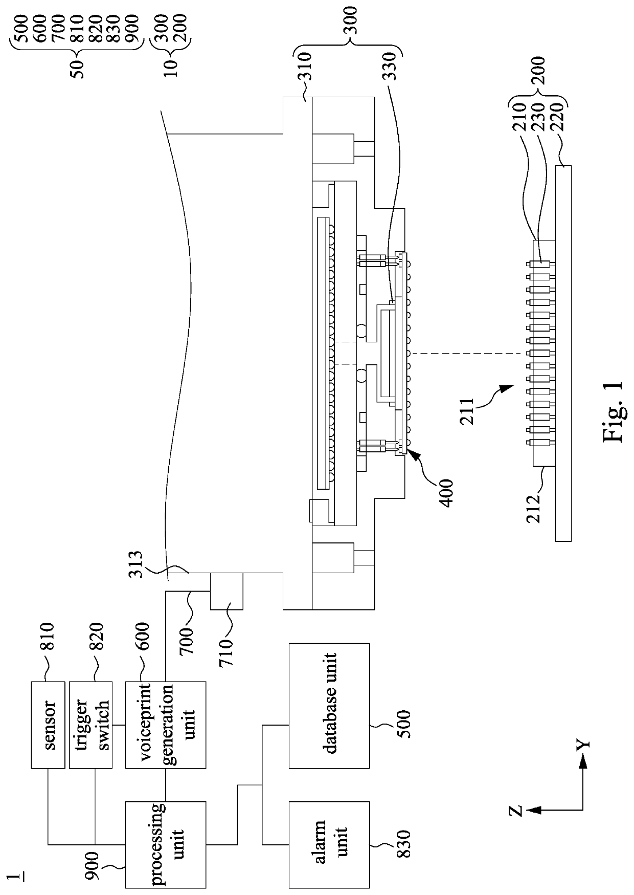
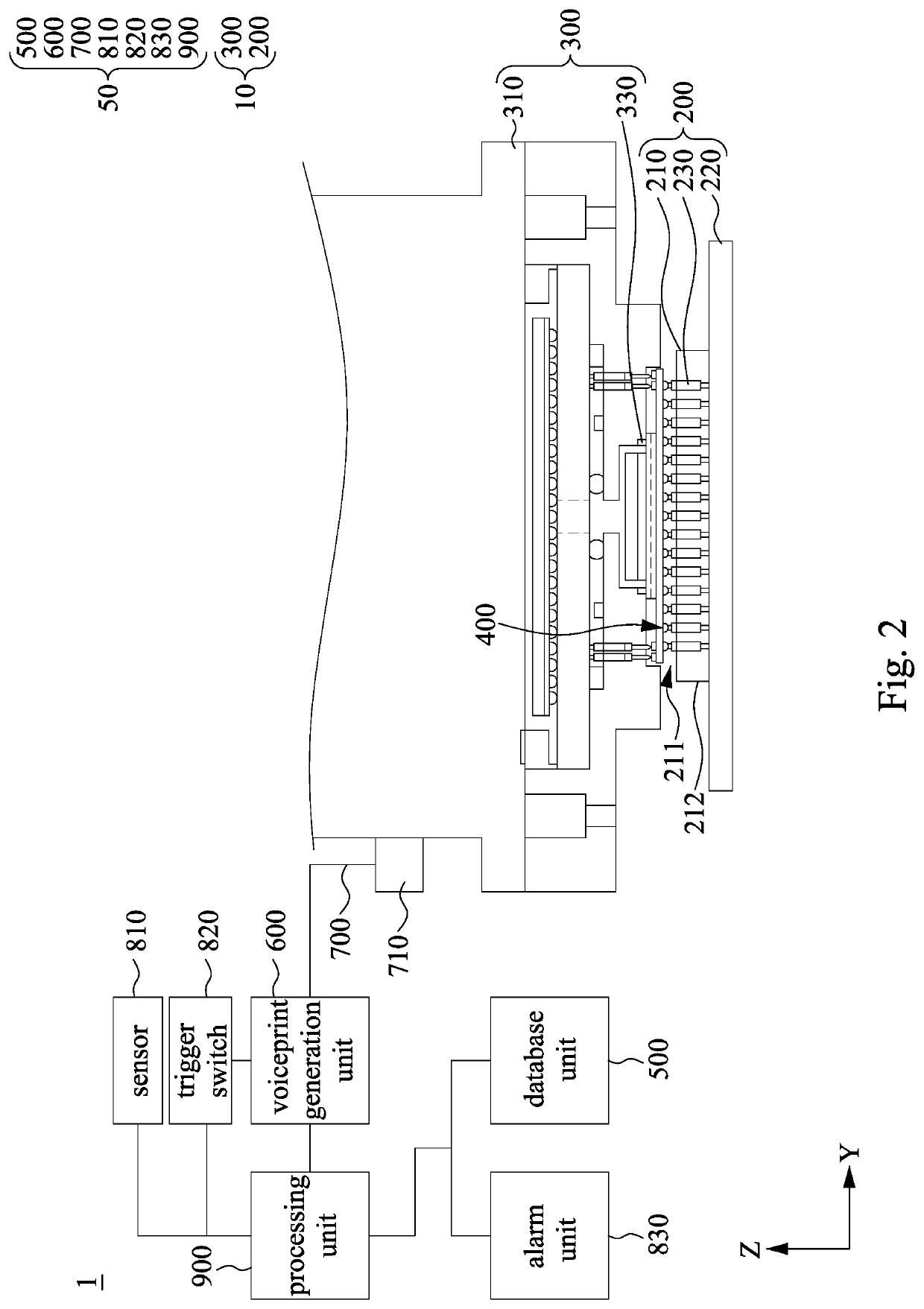
[0024]Reference is now made to FIG. 1 to FIG. 2, in which FIG. 1 is a schematic view of a testing system 1 according to one embodiment of the present disclosure, and FIG. 2 is an operational schematic view of the testing system 1 of FIG. 1. As shown in FIG. 1 and FIG. 2, the testing system 1 includes a testing apparatus 10 and a crack noise monitoring device 50. The testing apparatus 10 includes a testing stage 200 and an element pickup module 300. The element ...


PUM

PropertyMeasurementUnit
pressureaaaaaaaaaa
sound conductionaaaaaaaaaa
areaaaaaaaaaaa

Abstract

A testing system includes a testing apparatus and a crack noise monitoring device. The testing apparatus includes a testing stage and an element pickup module for pressing a semiconductor element on the testing stage. The crack noise monitoring device includes a database unit, a sound conduction set, a voiceprint generation unit and a processing unit. The database unit has a first voiceprint pattern. The sound conduction set is connected to the voiceprint generation unit and the testing apparatus for transmitting a sound wave from the semiconductor element to the voiceprint generation unit. The voiceprint generation unit receives and converts the sound wave into a second voiceprint pattern. The processing unit is electrically connected to the voiceprint generating unit and the database unit for determining whether the first voiceprint pattern is identical to the second voiceprint pattern.

Description

RELATED APPLICATIONS[0001]This application claims priority to Taiwan Application Serial Number 110109191, filed on Mar. 15, 2021, which is herein incorporated by reference.BACKGROUNDField of Disclosure[0002]The present disclosure relates to a testing system. More particularly, the present disclosure relates to a testing system capable of monitoring crack noise, a crack noise monitoring module and a method for monitoring crack noise.Description of Related Art[0003]With the rapid development of electronic technology and the appearance of high-tech electronical industries in recent years, electronic products with more user-friendly and better function are constantly introduced and designed in the trend of light and compact.[0004]However, when a semiconductor element (referred to a device under test, DUT) is pressed down on a testing area for a testing procedure, since the semiconductor device is caused to be damaged or cracked under pressure, a defective rate is often increased so as t...

Claims


Application Information

Patent Timeline
Patent Type & Authority Applications(United States)
IPC IPC(8): G10L25/51H04R1/34H04R1/08H04R1/28H04R19/04H04R7/04H04R7/16G08B3/10G01N29/14
CPCG10L25/51H04R1/342H04R1/08H04R1/2876H04R19/04H04R7/04H04R7/16G08B3/10G01N29/14H04R2201/003G01N2291/2697G01N29/225
Inventor LIAO, CHIH-CHIEHCHENG, CHIH-FENGSUN, YU-MIN
Owner GLOBAL UNICHIP CORPORATION
Why Eureka
Try Eureka