Semiconductor Component and Method for Producing the Same

Pending Publication Date: 2022-10-06
OSRAM OPTO SEMICON GMBH & CO OHG
View PDF0 Cites 0 Cited by
  • Summary
  • Abstract
  • Description
  • Claims
  • Application Information

AI Technical Summary

Benefits of technology

The patent describes a new method for producing an optoelectronic component with increased efficiency. The method involves using a filling layer made of a highly thermally conductive material to improve heat dissipation and allow for a higher operating current and more light output. The filling layer is transparent to the structured surface of the semiconductor body, allowing for improved heat conduction. The method also includes a polishing step where the surface is not perfectly flat, but can be made planar for easier attachment of a converter layer. An intermediate layer is used to minimize thermal resistance in the transition region between the semiconductor body and the converter layer. The method results in higher efficiency and reliability of the optoelectronic component.

Problems solved by technology

However, by roughening the semiconductor body to achieve a high out-coupling efficiency, thermal barriers can be formed that make it difficult to cool down a converter layer of the component.
However, this leads to a degradation of the optical out-coupling, since total reflection at a flat surface occurs more often when light shall pass to a material with a lower refractive index.
However, there is a high risk that the heat-conducting particles lead to undesired optical scattering, as a result of which out-coupled light is reflected back to the semiconductor body.

Method used


Image

  • Semiconductor Component and Method for Producing the Same
  • Semiconductor Component and Method for Producing the Same
  • Semiconductor Component and Method for Producing the Same

Examples


Embodiment Construction

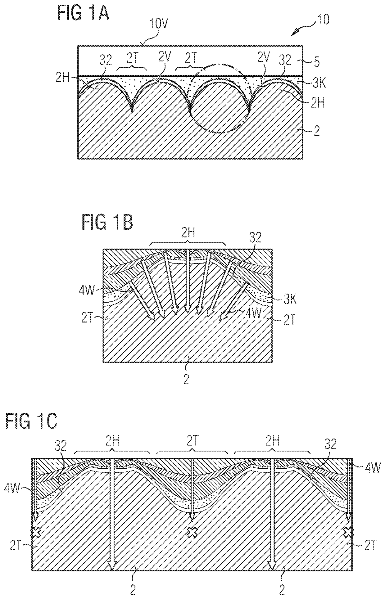
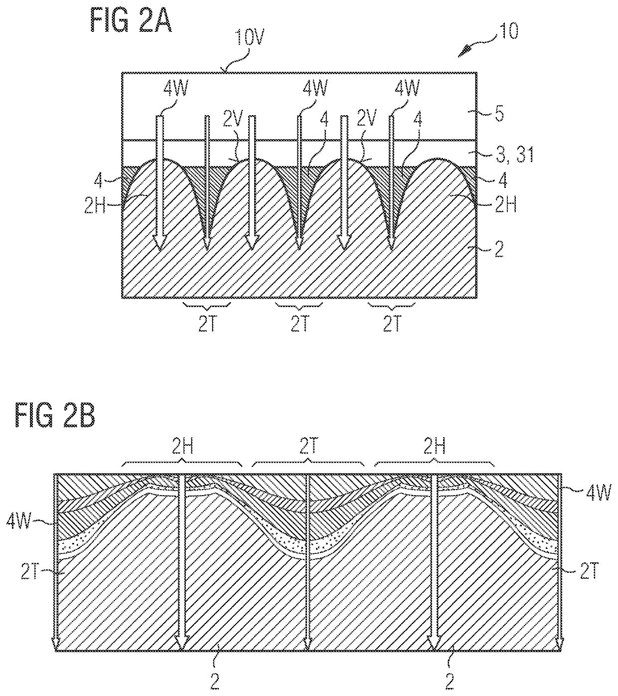
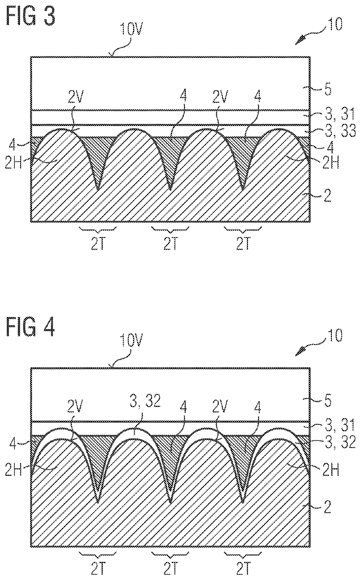
[0054]FIG. 1A shows a comparative example of a component 10 having a semiconductor body 2 and a converter layer 5, wherein the converter layer 5 is mechanically connected to the semiconductor body 2 by a connecting layer 3K. The semiconductor body 2 has a surface 2V which faces the converter layer 5, is formed in a structured manner and has recesses 2T and elevations 2H. The recesses 2T and the elevations 2H are provided with a passivation layer 32, wherein the passivation layer 32 runs substantially conformally with the structured surface 2V.

[0055]The component 10 is in particular a light-emitting component, for instance an LED chip, wherein the semiconductor body 2 is configured to generate electromagnetic radiation of first peak wavelength, which is scattered at the structured surface 2V during operation of the component and is coupled into the converter layer 5. In particular, the converter layer 5 contains phosphors that at least partially convert the radiation of first peak wa...


PUM


Abstract

In an embodiment a component includes a semiconductor body, a converter layer, a filling layer and an intermediate layer arranged in a vertical direction between the semiconductor body and the converter layer, wherein the semiconductor body has a surface which faces the converter layer, is structured and has vertical recesses, wherein the vertical recesses are filled with a material of the filling layer that has a higher thermal conductivity than silicone, wherein the intermediate layer or the semiconductor body has a higher mechanical hardness than the filling layer, and wherein the structured surface of the semiconductor body has local elevations and local recesses, the structured surface including exclusively the surface of an n-type or a p-type semiconductor layer.

Description

[0001]This patent application is a national phase filing under section 371 of PCT / EP2020 / 071528, filed Jul. 30, 2020, which claims the priority of German patent application 102019121678.8, filed Aug. 12, 2019, each of which is incorporated herein by reference in its entirety.TECHNICAL FIELD[0002]A component having improved heat dissipation and thus having improved efficiency is specified. Furthermore, a method for producing a component is specified.BACKGROUND[0003]The efficiency and lifetime of a light-emitting component depend, among other things, on whether heat of the component is sufficiently dissipated during operation. Often, a converter layer is attached to a structured surface of a semiconductor body of the component by a silicone-based connecting layer. However, by roughening the semiconductor body to achieve a high out-coupling efficiency, thermal barriers can be formed that make it difficult to cool down a converter layer of the component. Such thermal barriers are locate...

Claims


Application Information

Patent Timeline
IPC IPC(8): H01L33/64H01L33/20H01L33/44H01L33/50
CPCH01L33/641H01L33/20H01L33/44H01L33/50H01L2933/0025H01L2933/0041H01L2933/0075H01L33/642H01L33/505
Inventor TANGRING, IVAR
Owner OSRAM OPTO SEMICON GMBH & CO OHG
Why Eureka
Try Eureka