Light-emitting device, display device, imaging device, and electronic device

Pending Publication Date: 2022-10-06
CANON KK
View PDF0 Cites 0 Cited by
  • Summary
  • Abstract
  • Description
  • Claims
  • Application Information

AI Technical Summary

Benefits of technology

The invention makes it easier for a device to resist moisture.

Problems solved by technology

Light of a wide spectrum specific to the organic material is emitted in a light-emitting element that utilizes an organic light-emitting material; accordingly, it becomes difficult to obtain light of high color purity, and the color gamut (color reproduction range) of the obtained light is narrower.
As is known, organic compounds of light-emitting materials used in organic EL elements generally have low moisture resistance, and dark spots and leakage current occur on account of moisture that intrudes from outside.
In a connection portion having a conventional configuration, however, a problem arises in the form of poorer sealing performance for instance in that the transparent electrode constitutes a moisture intrusion route.

Method used


Image

  • Light-emitting device, display device, imaging device, and electronic device
  • Light-emitting device, display device, imaging device, and electronic device
  • Light-emitting device, display device, imaging device, and electronic device

Examples


embodiment 1

[0022]Embodiment 1 of the present invention will be explained next. An example in which the present invention is applied to a display device will be explained below, but the invention can also be applied to various devices such as light-emitting devices.

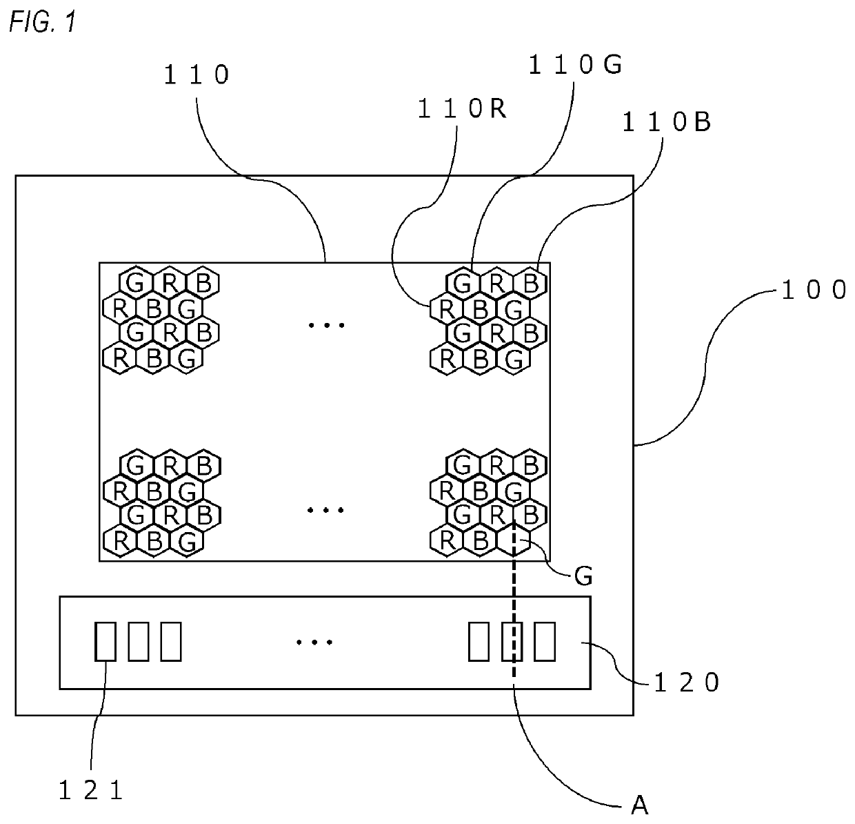
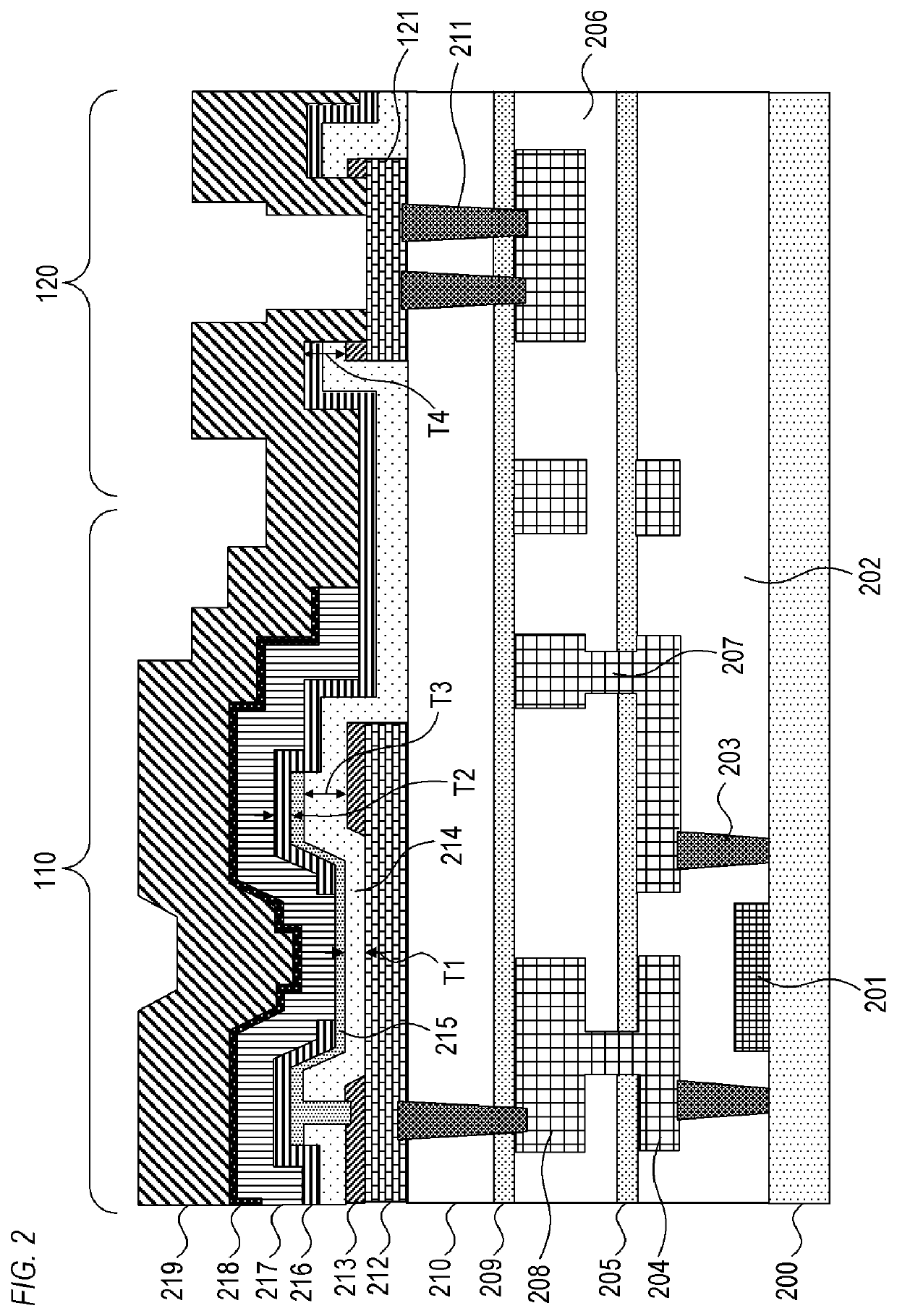
[0023]FIG. 1 is a plan-view diagram illustrating the structure of a display device 100 according to the present embodiment. The display device 100 has a pixel arrangement area 110 (element area) and a pad arrangement area 120 (terminal area) on a silicon substrate 200 (on a substrate). Sub-pixels 110R, 110G, 110B for display of red (R), green (G) and blue (B) are disposed in the pixel arrangement area 110, with respective light-emitting elements being disposed on the sub-pixels 110R, 110G, 110B. The arrangement of the sub-pixels can be for instance of delta type, such as that illustrated in FIG. 1, but may of mosaic type, of stripe type or of Bayer type. The pad arrangement area 120 is disposed in the periphery of the pixel arrangeme...

embodiment 3

[0059]Embodiment 3 of the present invention will be explained next. In the present embodiment examples will be explained in which the present invention is applied to various devices.

[0060]FIG. 8 is a schematic diagram illustrating a display device 1000 being an example of a display device according to the present embodiment. The display device 1000 may have a touch panel 1003, a display panel 1005, a frame 1006, a circuit board 1007 and a battery 1008, between an upper cover 1001 and a lower cover 1009. The display panel 1005 is a display panel (display unit) to which the present invention is applied. For instance the display panel 1005 has a light-emitting device having a structure such as that illustrated in FIG. 2, FIG. 5 or FIG. 6, and displays images using the light emitted from the light-emitting device. Flexible printed circuit FPCs 1002, 1004 are connected to the touch panel 1003 and the display panel 1005. A control circuit including transistors is printed on the circuit bo...


PUM


Abstract

A light-emitting device according to the present invention includes, on a substrate, an element area in which a light-emitting element is disposed, and a terminal area in which a terminal portion electrically connected to the light-emitting element is disposed, wherein the light-emitting element has, sequentially from the substrate, a reflective layer, a first insulating layer, a first electrode, a second insulating layer, an organic layer that includes a light-emitting layer, a second electrode, and a third insulating layer, the terminal portion has a pad electrode of a material identical to that of the reflective layer, the pad electrode has an exposed portion at which a surface on a far side from the substrate is exposed, and the third insulating layer extends from the element area up to an edge of the exposed portion in the terminal area.

Description

BACKGROUND OF THE INVENTIONField of the Invention[0001]The present invention relates to a light-emitting device, a display device, an imaging device, and an electronic device.Description of the Related Art[0002]Organic electronic elements that utilize organic compounds have been studied in recent years. In particular, organic light-emitting devices, also called organic electroluminescence elements or organic EL elements, are being developed at a rapid pace.[0003]In order to implement full color in display devices it is necessary to obtain light of three primary colors, red (R), green (G) and blue (B). Methods for obtaining the three primary colors RGB in a case where an organic light-emitting element is used as a light source include a method in which respective light-emitting layers that emit red, green and blue light are applied separately, and a method in which color separation is accomplished using a white light-emitting element and RGB color filters. Light of a wide spectrum sp...

Claims


Application Information

Patent Timeline
IPC IPC(8): H01L51/52H01L27/32
CPCH01L51/5271H01L27/3276H01L27/3234H10K59/123H10K59/124H10K59/122H10K59/131H10K50/852H10K50/844H10K59/65H10K50/84H10K50/856
Inventor SUZUKI, KENTARO
Owner CANON KK
Why Eureka
Try Eureka