

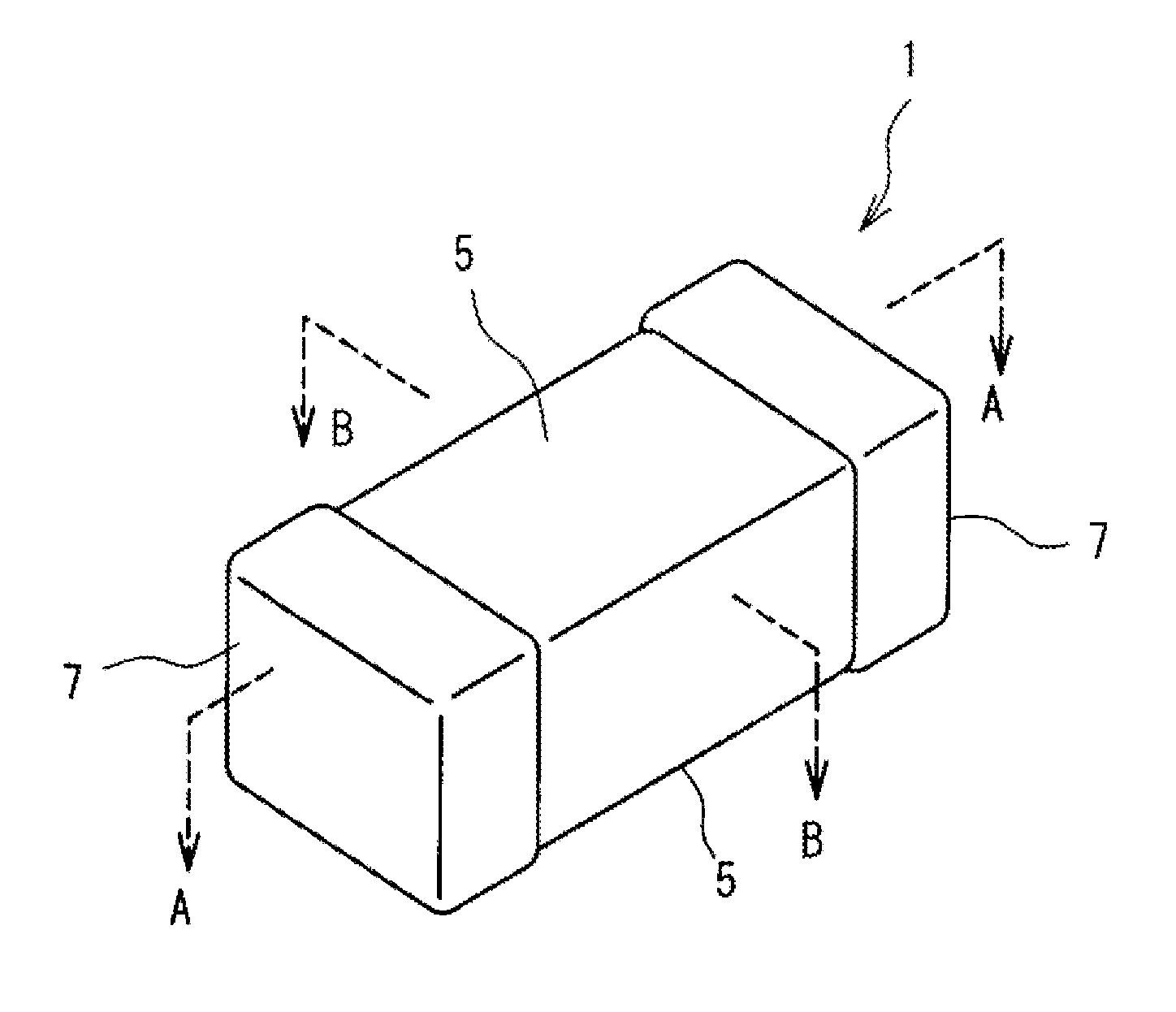
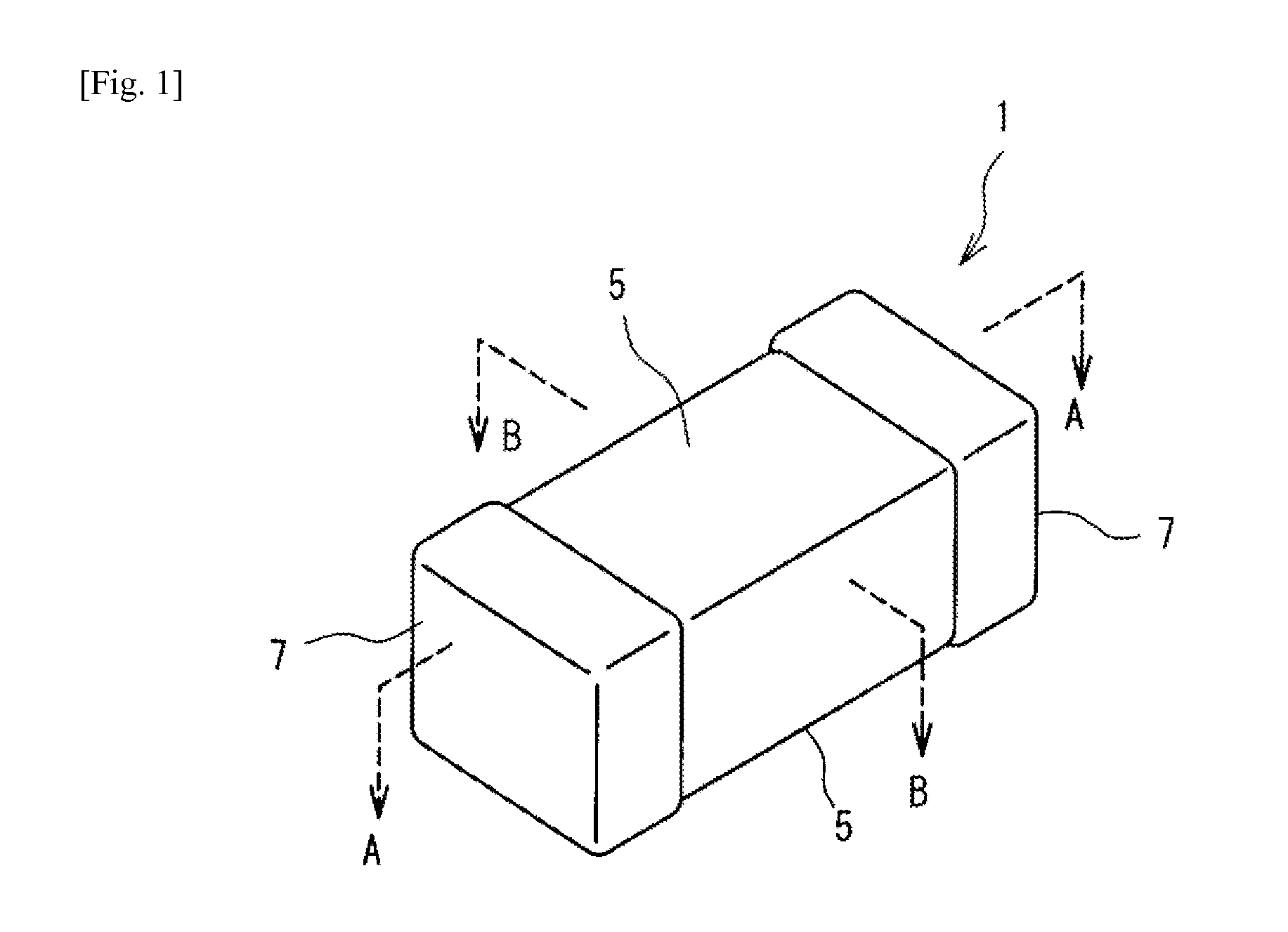
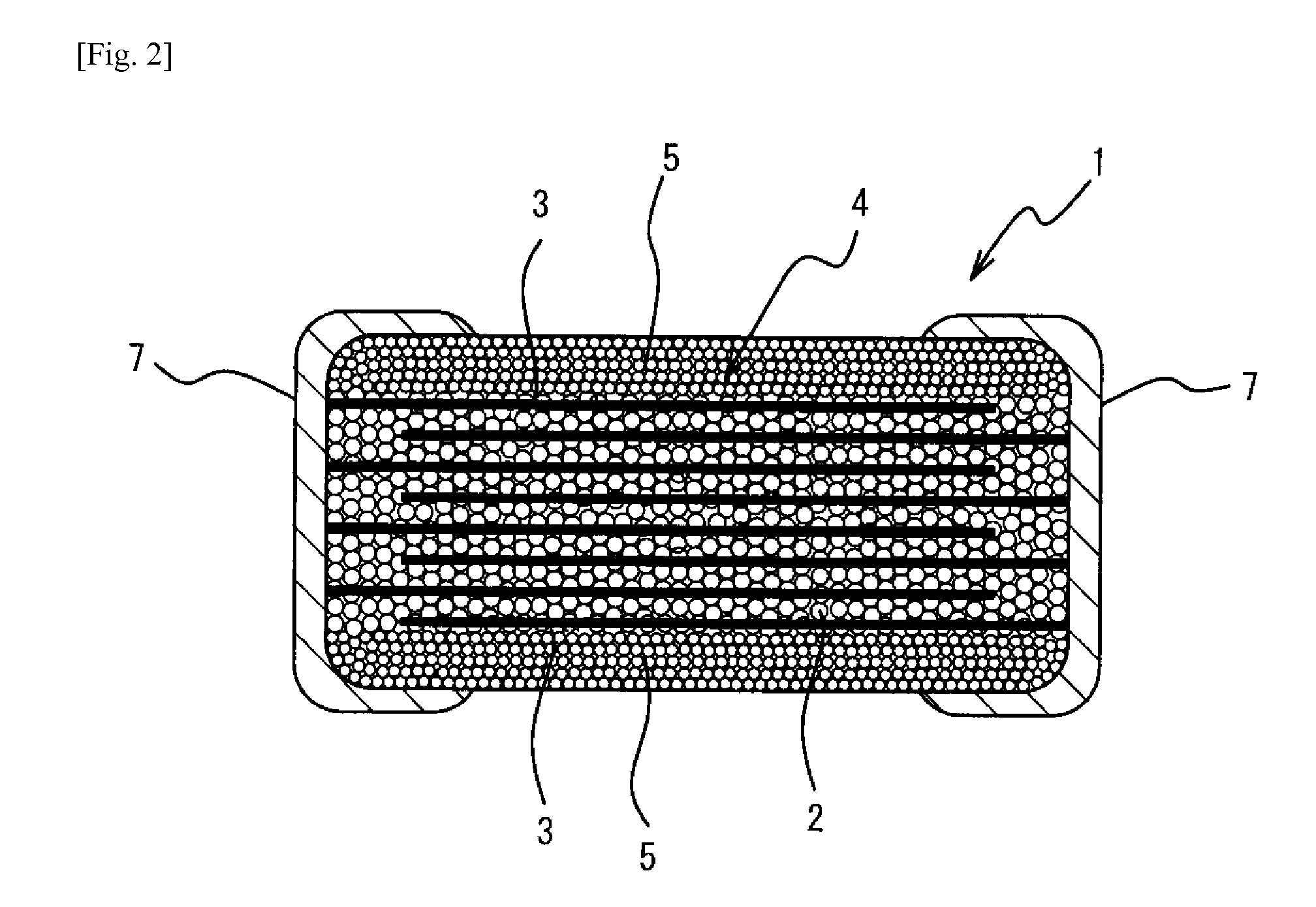
Laminated ceramic capacitor
- Summary
- Abstract
- Description
- Claims
- Application Information
AI Technical Summary
Benefits of technology
Problems solved by technology
Method used
Image

Examples
example 1
[0034]A ceramic green sheet constituted by a dielectric material of 0.225 μm in average grain size whose main ingredient is BaTiO3, and a binder, was prepared, and a Ni conductive paste was applied onto this sheet by means of screen printing, to form band-shaped paste films arranged at a specified pitch. A plurality of printed ceramic green sheets were prepared and stacked on top of one another in such a way that the band-shaped paste films were overlapped in a manner offset by one-half pattern. A ceramic green sheet on which a conductive paste had not been printed was placed as a cover layer on top and bottom of the stacked ceramic green sheets. This stack of ceramic green sheets was pressure-bonded and cut to a specified chip size to obtain an unsintered laminate block having a pair of cover layers. A ceramic paste constituted by a dielectric material of 0.200 μm in average grain size and a binder, was applied to both side faces of this laminate block, to form ceramic bodies. Next...
example 2
[0036]A total of 100 laminated ceramic capacitor samples #2 were produced in the same manner as in Example 1, except that the ceramic bodies were formed using a ceramic paste constituted by a dielectric material of 0.170 μm in average grain size and a binder.
[0037]The laminated ceramic capacitor samples #2 produced as above were soaked for 3 seconds in a molten solder of 400° C. to check if cracks were generated. As a result, none of the laminated ceramic capacitor samples #2 generated cracks.
example 3
[0038]A total of 100 laminated ceramic capacitor samples #3 were produced in the same manner as in Example 1, except that the ceramic bodies were formed using a ceramic paste constituted by a dielectric material of 0.135 μm in average grain size and a binder.
[0039]The laminated ceramic capacitor samples #3 produced as above were soaked for 3 seconds in a molten solder of 400° C. to check if cracks were generated. As a result, none of the laminated ceramic capacitor samples #3 generated cracks.
PUM
| Property | Measurement | Unit |
|---|---|---|
| Grain size | aaaaa | aaaaa |
| Grain size | aaaaa | aaaaa |
| Fraction | aaaaa | aaaaa |
Abstract
Description
Claims
Application Information