Nitride-based electronic device and method for manufacturing same

Active Publication Date: 2019-09-26
WAVICE INC
View PDF2 Cites 0 Cited by
  • Summary
  • Abstract
  • Description
  • Claims
  • Application Information

AI Technical Summary

Benefits of technology

The present invention relates to a nitride-based electronic device and method of manufacturing it. The invention uses a plurality of passivation layers and resin layers to form a structure that prevents moisture from exposing the ends of the layers. This improves moisture resistance without the need for a separate opening. Additionally, the invention prevents a region between layers and the upper portion of electrode pad from being exposed, further improving moisture resistance. The technical effects of this invention are improved reliability and durability of electronic devices.

Problems solved by technology

However, a volume of the resin film may be changed due to changes in humidity and temperature, and the change in the volume of the resin film may cause a portion of a nitride-based lower protection layer to be delaminated.
Moisture may permeate into the delaminated portion of the protection layer, and surfaces of metal electrode pads may be easily oxidized due to the permeation of the moisture, which may lower the stability and reliability of the nitride-based electronic device which uses a high voltage.
Even if an opening irrespective of the exposure of the drain electrode pad is formed in the resin film in order to prevent the protection layer from being delaminated due to a change in volume of the resin film, fine moisture may be introduced into a gap between thin films, which results in a decrease in the stability and reliability of the device.
In addition, when the opening which exposes the drain electrode pad and the opening which prevents delamination of the protection layer are formed, due to an etch stop difference, it is very difficult to concurrently form the two openings having substantially different functions.
That is, an etch stop of the opening which exposes the drain electrode pad is a drain electrode pad made of a metal, and the opening which prevents the delamination of the protection layer becomes a protection layer made of a nitride, and thus, a manufacturing process is not easy.
Therefore, the two openings should be formed using separate photolithography processes, resulting in an increase in the number of process operations.

Method used


Image

  • Nitride-based electronic device and method for manufacturing same
  • Nitride-based electronic device and method for manufacturing same
  • Nitride-based electronic device and method for manufacturing same

Examples


first exemplary embodiment

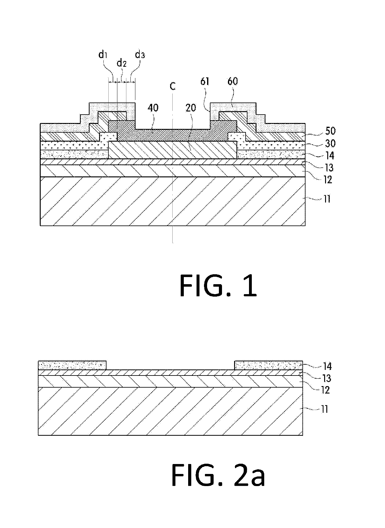
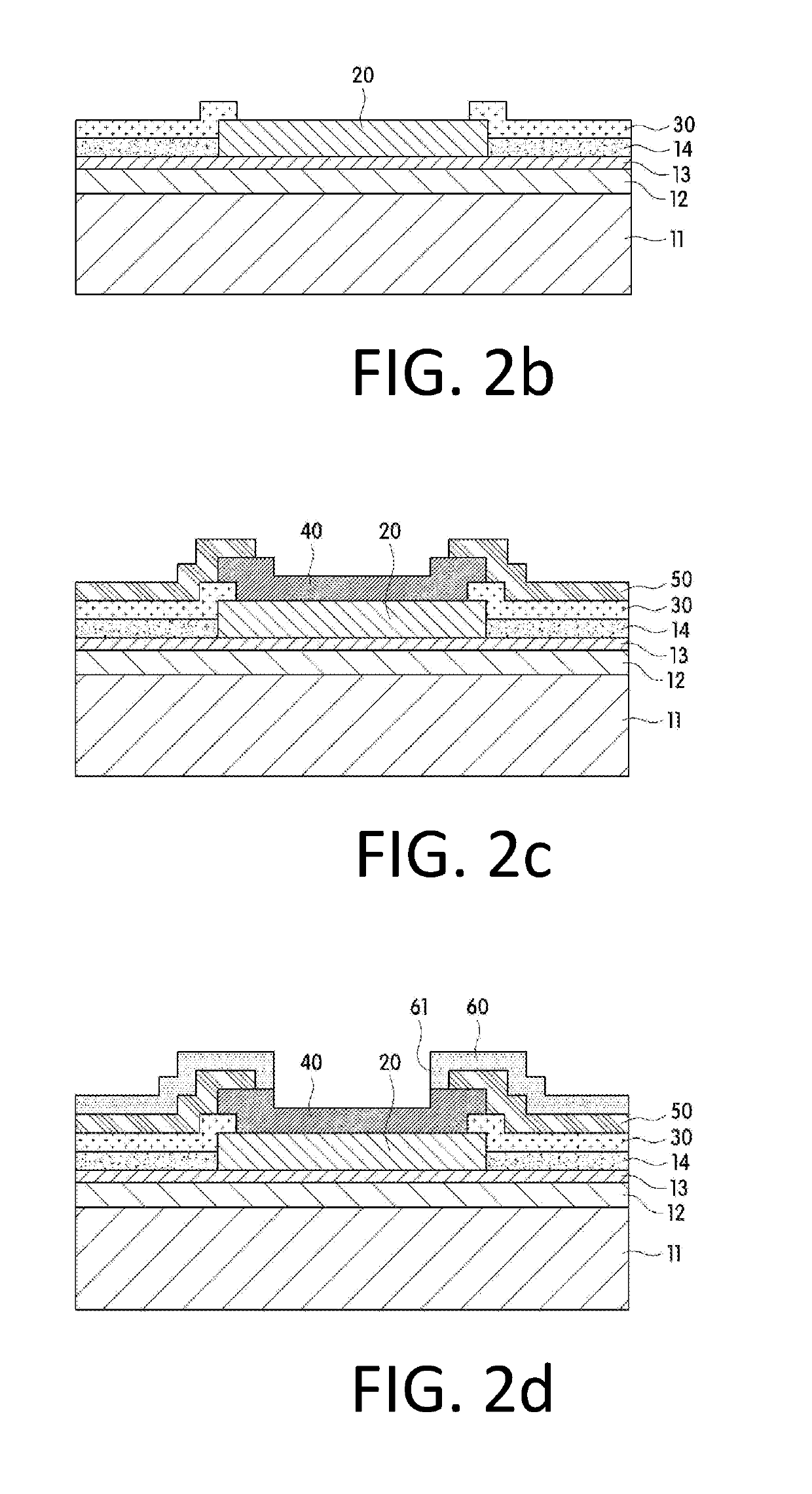
[0038]FIG. 1 is a cross-sectional view illustrating a part of a nitride-based electronic device according to a first exemplary embodiment of the present invention.

[0039]As shown in FIG. 1, the nitride-based electronic device according to the first exemplary embodiment includes a substrate 11, a channel layer 12 formed on the substrate 11, a barrier layer 13 formed on the channel layer 12, a first protection layer 14 disposed on the barrier layer 13 to expose a partial region of the barrier layer 13, a drain electrode 20 disposed on the barrier layer 13 exposed by the first protection layer 14, a second protection layer 30 disposed to cover an entire upper surface of the first protection layer 14 and a partial peripheral portion of an upper surface of the drain electrode 20, a drain electrode pad 40 disposed on the upper surface of the drain electrode 20 and a portion of the second protection layer 30 on the peripheral portion of the drain electrode 20, a third protection layer 50 co...

second exemplary embodiment

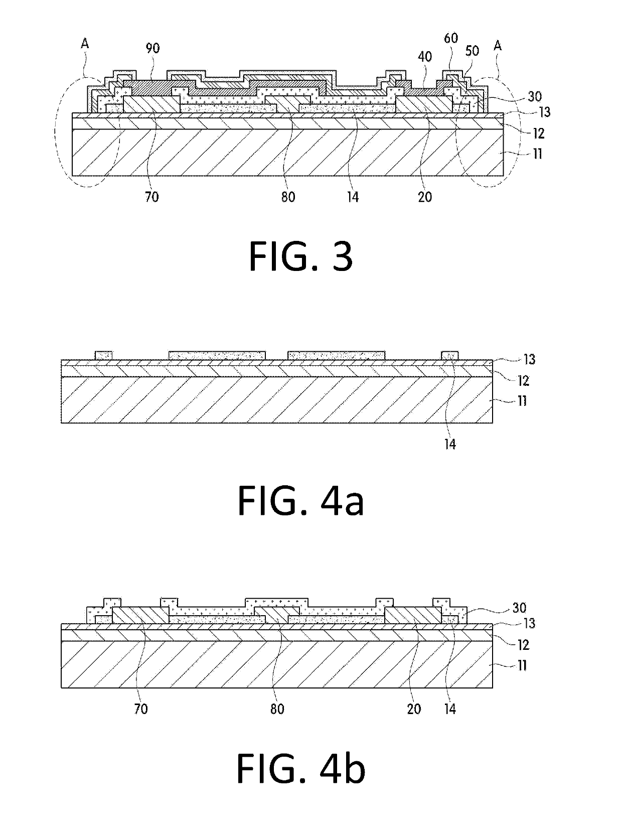
[0065]FIG. 3 is a cross-sectional view illustrating a nitride-based electronic device according to a second exemplary embodiment of the present invention.

[0066]Referring to FIG. 3, the nitride-based electronic device according to the second exemplary embodiment of the present invention is illustrated as further including a source electrode 70, a gate electrode 80, and a field plate 90 unlike the first exemplary embodiment shown in FIG. 1

[0067]FIG. 3 shows that, in a stacked structure of multiple protection layers, which is a characteristic configuration of the present invention, structures of upper protection layers, which completely cover protection layers disposed thereunder, are not limited to being formed on a drain electrode pad.

[0068]It may be understood that the field plate 90, which is in contact with an upper portion of the source electrode 70 and extends to an upper portion of a third protection layer 50 above the gate electrode 80, also functions as a source electrode pad...


PUM


Abstract

The present invention relates to a nitride-based electronic device and a method for manufacturing same, the nitride-based electronic device comprising a substrate, a metal electrode and a plurality of protection layers, wherein, among the protection layers, at least two protection layers covering one portion of the electrode so that one portion of the upper part of the electrode is exposed are configured so that the upper protection layer covers the end part of the lower protection layer so as to prevent the end part of the lower protection layer from being exposed.

Description

TECHNICAL FIELD[0001]The present invention relates to a nitride-based electronic device and a method of manufacturing the same, and more particularly, to a nitride-based electronic device in which stability and reliability may be improved, and a method of manufacturing the same.BACKGROUND ART[0002]Generally, nitride-based electronic devices have a broad energy band gap, high thermal and chemical stability, and a high electron saturation velocity as compared with common semiconductor materials such as Si and GaAs. The nitride-based electronic devices are known to be suitable for high frequency and high capacity applications.[0003]In the nitride-based electronic device, a channel layer and a barrier layer, which are different nitride layers, may be stacked to provide a large band discontinuity at a junction interface, and high concentration electrons may be induced due to the large band discontinuity, thereby improving electron mobility.[0004]In the nitride-based electronic devices ha...

Claims


Application Information

Patent Timeline
IPC IPC(8): H01L23/00H01L29/20H01L29/205H01L29/40H01L29/778H01L23/29H01L23/31H01L21/02H01L21/311H01L21/765H01L29/66
CPCH01L29/7787H01L29/205H01L21/765H01L23/293H01L29/402H01L21/31133H01L29/66462H01L21/02118H01L23/564H01L23/3192H01L29/2003H01L21/768H01L21/225H01L29/7786H01L23/291H01L23/3171H01L2224/02166H01L2224/05H01L2224/02126H01L29/778H01L21/2254H01L21/76885H01L21/76829H01L21/76841
Inventor LEE, SANG MINKOO, HWANG SUBKIM, HYUN JEJUNG, HEE SEOK
Owner WAVICE INC
Why Eureka
Try Eureka