Linearity test system, linearity signal providing device, and linearity test method
- Summary
- Abstract
- Description
- Claims
- Application Information
AI Technical Summary
Benefits of technology
Problems solved by technology
Method used
Image

Examples
first embodiment
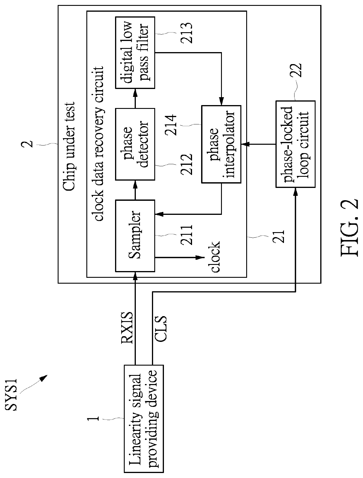
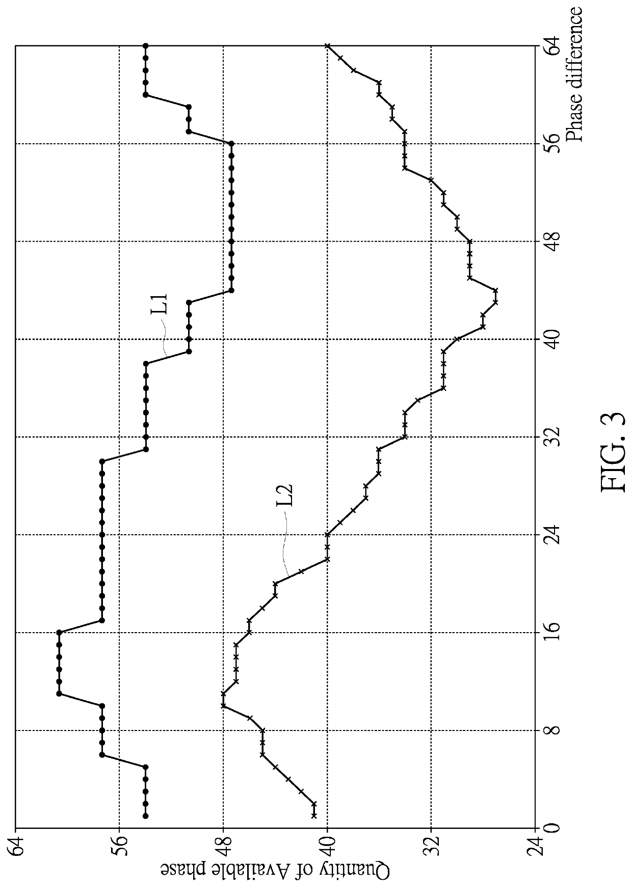
[0020]A linearity signal providing device of the present disclosure provides a reference clock signal and a receiver input signal at the same time, and outputs the reference clock signal and the receiver input signal that have a phase difference in time domain to a chip. A jitter tolerance test is processed to obtain available phases of the chip. When the linearity of the chip is good, the available phases of the two signals having phase differences in time domain are similar. When the linearity of the chip is bad, quantities of the available phases of the two signals having phase differences in time domain are different.
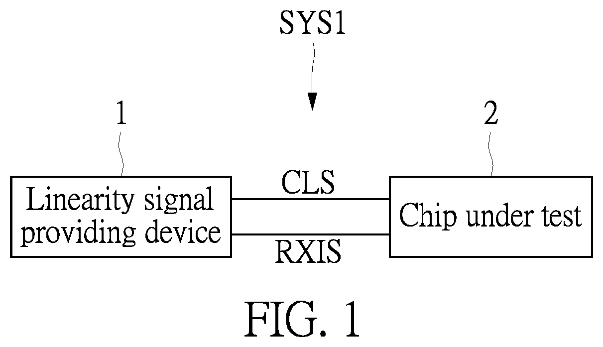
[0021]Referring to FIG. 1, FIG. 2, and FIG. 3, FIG. 1 is a schematic view of a linearity test system for a chip according to a first embodiment of the present disclosure. FIG. 2 is another schematic view of the linearity test system for the chip according to the first embodiment of the present disclosure. FIG. 3 is a schematic view of a jitter tolerance test of the ...
second embodiment
[0032]Referring to FIG. 4, FIG. 4 is a schematic view of a linearity signal providing device according to a second embodiment of the present disclosure
[0033]The linearity signal providing device 1 includes a controller 11, a first signal generation circuit 12, a second signal generation circuit 13, a data delay circuit 14, a first output circuit 15, and a second output circuit 16.
[0034]The controller 11 is electrically connected to the first signal generation circuit 12 and the second signal generation circuit 13. The first signal generation circuit 12 is electrically connected to the first output circuit 15. The second signal generation circuit 13 is electrically connected to the data delay circuit 14. The data delay circuit 14 is electrically connected to the second output circuit 16.
[0035]The first signal generation circuit 12 is configured to generate the reference clock signal CLS. The second signal generation circuit 13 is configured to generate the receiver input signal RXIS....
third embodiment
[0037]Referring to FIG. 5, FIG. 5 is a schematic view of a linearity test method for the chip according to a third embodiment of the present disclosure.
[0038]The method for testing a linearity of a chip is adapted to the linearity test system for the chip SYS1 of the first embodiment and the linearity signal providing device 1 of the second embodiment, and it is not limited thereto. The structure and the function of the linearity test system for the chip SYS1 and the linearity signal providing device 1 is omitted herein.
[0039]The linearity test method of the chip includes following steps:
[0040]providing a reference clock signal and a receiver input signal that have a phase difference in time domain (step S110); and
[0041]determining a linearity of a phase interpolator of a chip under test based on a plurality of phase signals corresponding to the reference clock signal and the receiver input signal transmitted in the chip under test (step S120).
[0042]In step S110, the linearity test ...
PUM
 Abstract
Description
Claims
Application Information
 - R&D Engineer
- R&D Manager
- IP Professional
- Industry Leading Data Capabilities
- Powerful AI technology
- Patent DNA Extraction
Browse by: Latest US Patents, China's latest patents, Technical Efficacy Thesaurus, Application Domain, Technology Topic.
© 2024 PatSnap. All rights reserved.Legal|Privacy policy|Modern Slavery Act Transparency Statement|Sitemap