Imaging device and image processing method

Pending Publication Date: 2022-11-17
PANASONIC INTELLECTUAL PROPERTY MANAGEMENT CO LTD
View PDF4 Cites 0 Cited by
  • Summary
  • Abstract
  • Description
  • Claims
  • Application Information

AI Technical Summary

Benefits of technology

[0004]One non-limiting and exemplary embodiment provides an imaging device and

Problems solved by technology

However, in a situation in which the solid-state imaging elements are actually used,

Method used


Image

  • Imaging device and image processing method
  • Imaging device and image processing method
  • Imaging device and image processing method

Examples


first embodiment

[0060]First, a description will be given of an imaging device according to a first embodiment.

Overall Configuration of Imaging Device

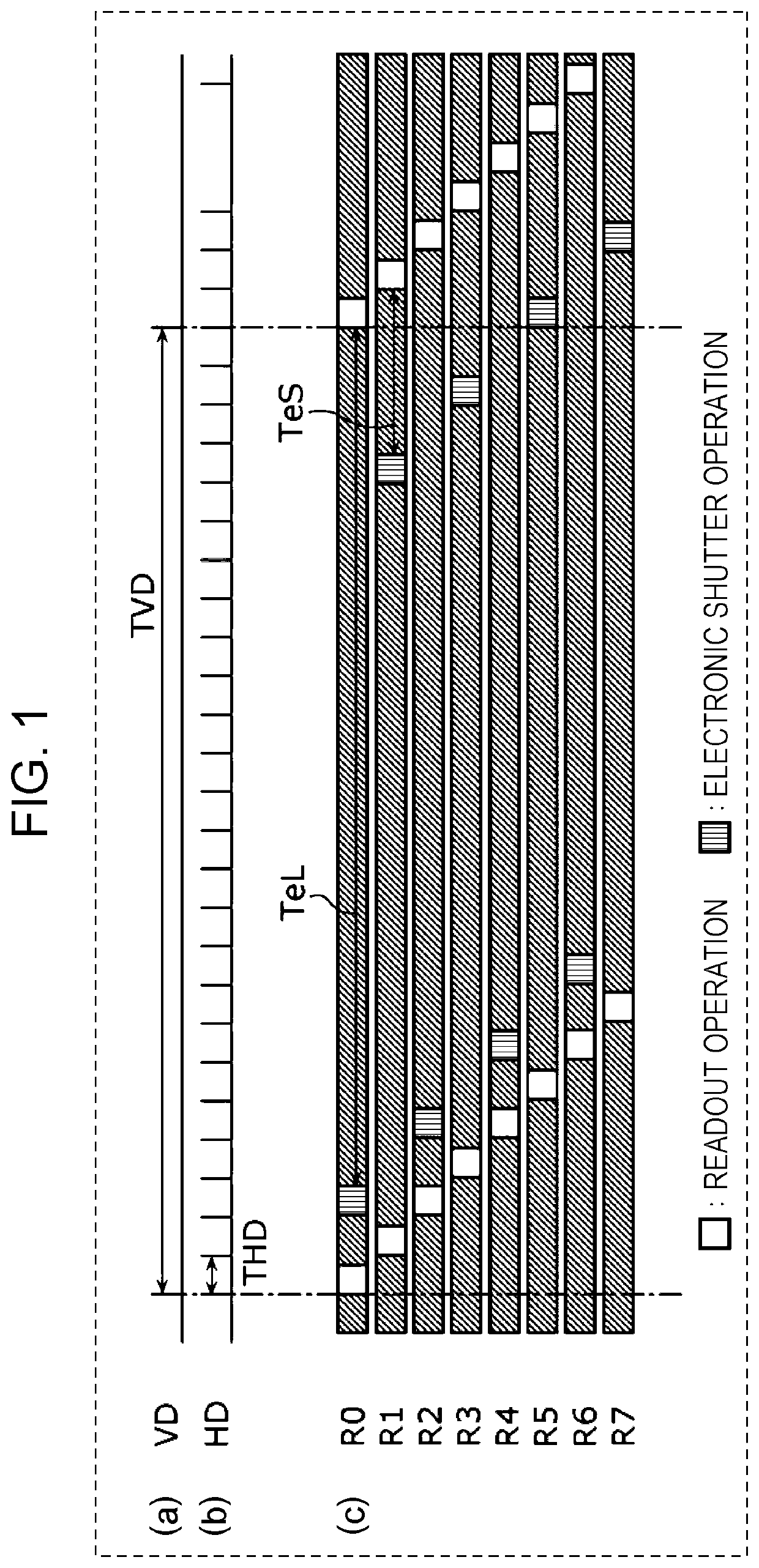
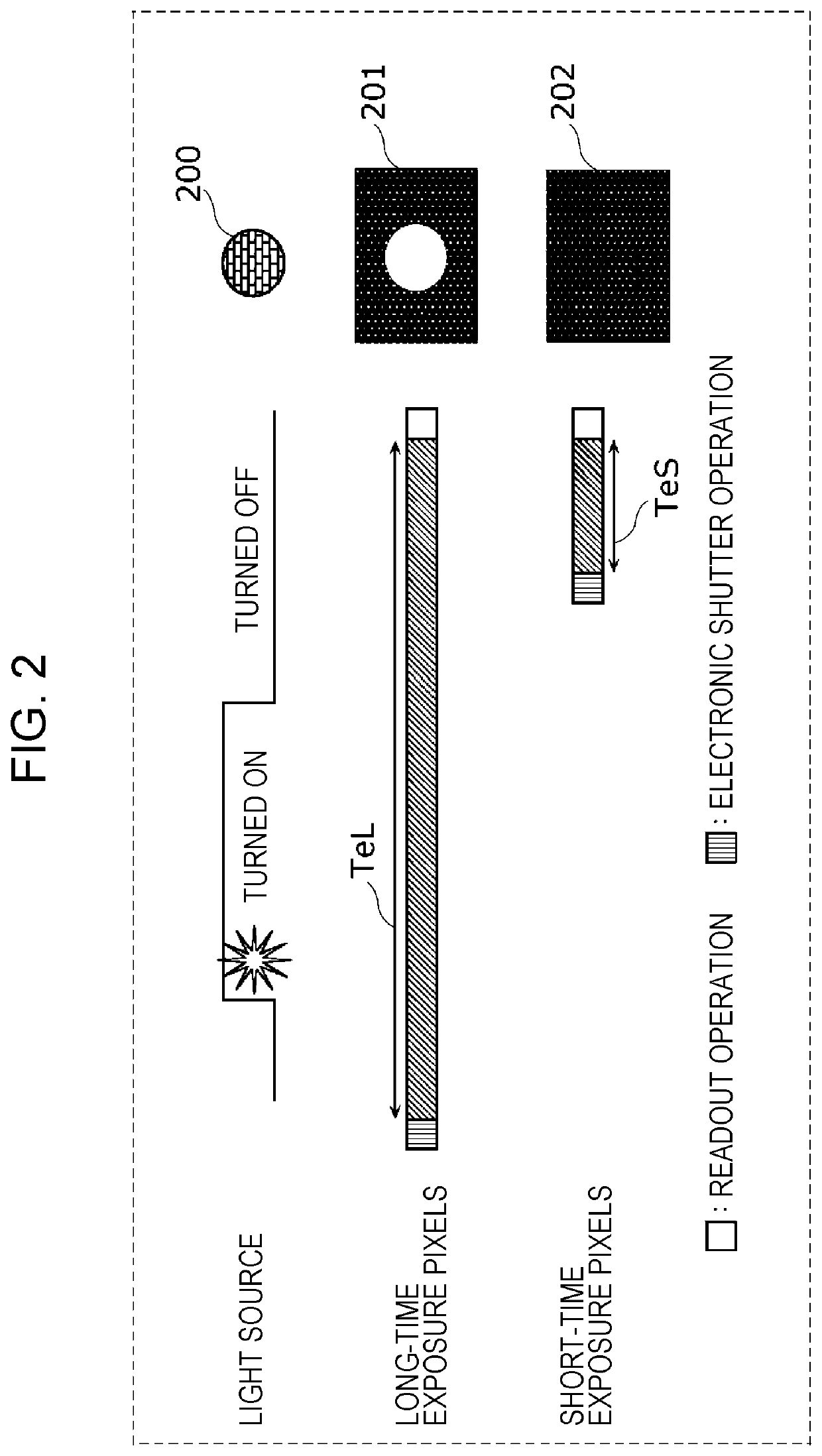
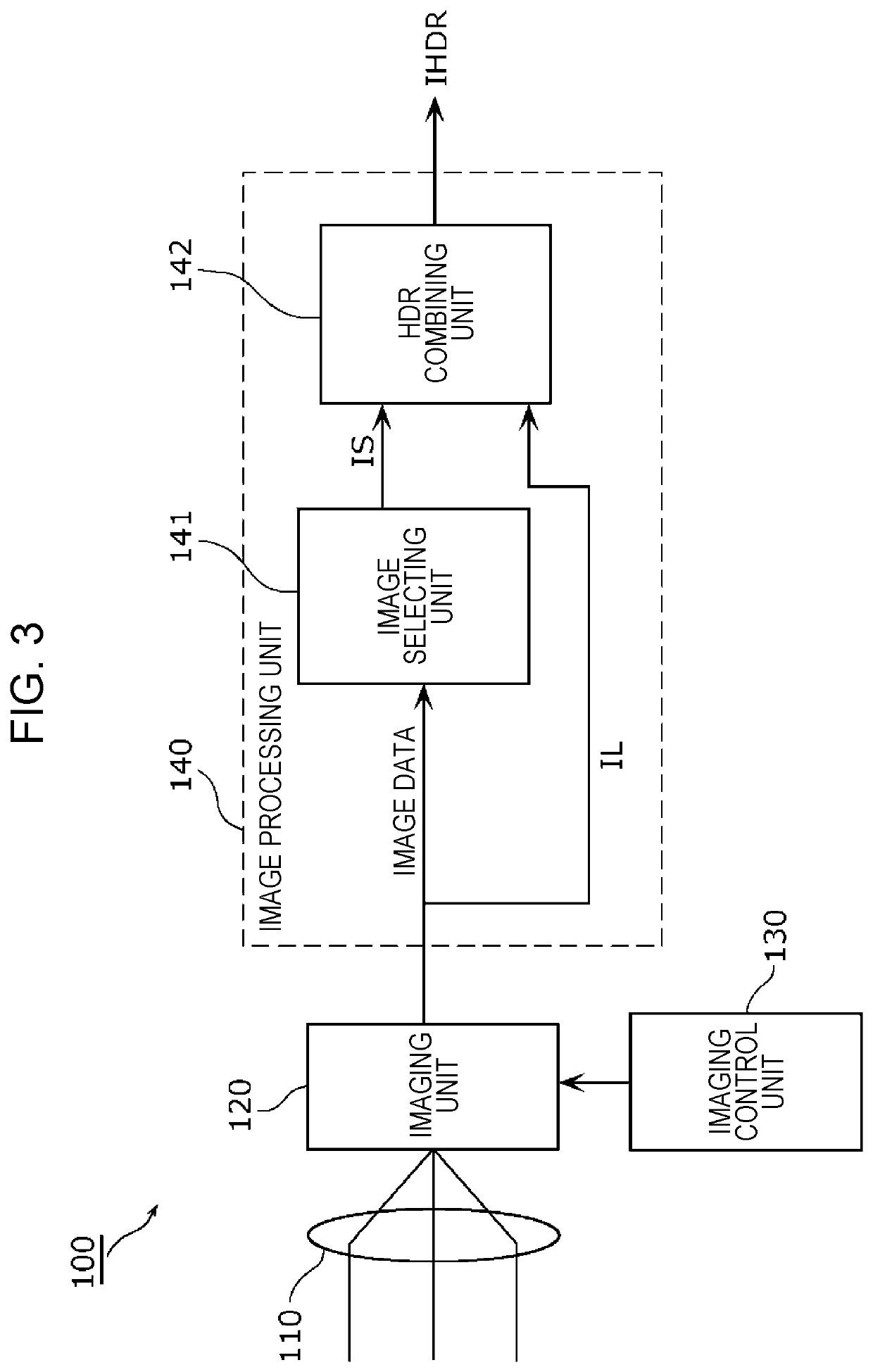
[0061]The imaging device according to the present embodiment has a function for generating image data of a high dynamic range image by using a plurality of pieces of image data resulting from imaging with different exposure times. An imaging unit included in the imaging device according to the present embodiment performs imaging with a predetermined exposure time and also reads out pixel signals nondestructively a plurality of times in the exposure time. In addition, an image processing unit included in the imaging device according to the present embodiment generates difference image data between a plurality of pieces of image data obtained by those nondestructive pixel-signal readouts. One piece of image data is selected from image data obtained first and the difference image data, for example, based on local luminance values in the pieces of image da...

second embodiment

[0165]Next, a description will be given of a second embodiment. The second embodiment differs from the above-described first embodiment in that an image selecting unit 141B is provided instead of the image selecting unit 141 provided in the imaging device 100.

[0166]FIG. 14 is a block diagram illustrating an exemplary configuration of the image selecting unit 141B according to the present embodiment. Compared with the image selecting unit 141 according to the first embodiment, the image selecting unit 141B differs in that it has a selection control unit 1408. Other constituent elements that are substantially the same as those in the image selecting unit 141 according to the first embodiment are denoted by reference numerals that are the same as those in FIG. 8, and detailed descriptions are not given hereinafter. Also, the operation of the image selecting unit 141B is mostly the same as the operation of the image selecting unit 141 according to the first embodiment illustrated in FIG...

third embodiment

[0174]Next, a description will be given of a third embodiment. The third embodiment differs from the first embodiment in that an imaging unit 120B is provided instead of the imaging unit 120 provided in the imaging device 100. The photoelectric converters 13 are not limited to those having the photoelectric conversion layers 15 as illustrated in FIGS. 4 and 5. For example, photodiodes (PD) may be used as the photoelectric converters.

[0175]FIG. 16 is a schematic diagram illustrating an exemplary circuit configuration of the imaging unit 120B according to the present embodiment. Constituent elements that are substantially the same as those in the imaging unit 120 in the first embodiment illustrated in FIG. 4 are denoted by references numerals that are the same as in FIG. 4, and descriptions thereof are not given hereinafter.

[0176]As illustrated in FIG. 16, the imaging unit 120B has a pixel array PAB including a plurality of pixels 10B arranged two-dimensionally. Each pixel 10B has a p...


PUM


Abstract

An imaging device includes an imaging unit including a plurality of pixels, respectively including photoelectric converters and charge accumulation nodes that accumulate signal charge. The imaging unit outputs image data based on signals corresponding to the signal charge accumulated in the charge accumulators. The imaging device includes an image processing unit that processes the image data output by the imaging unit. The imaging unit sequentially outputs a plurality of pieces of image data in one frame period by performing readout nondestructively. The image processing unit generates difference image data by determining a difference between two pieces of image data, selects output image data from initial image data and the difference image data, and combines the output image data and normal readout image data included in the plurality of pieces of image data, to generate combination-result image data.

Description

BACKGROUND1. Technical Field[0001]The present disclosure relates to an imaging device and an image processing method.2. Description of the Related Art[0002]In recent years, charge-coupled device (CCD) sensors, complementary metal-oxide semiconductor (CMOS) sensors, and so on have come into widespread use as solid-state imaging elements for imaging devices that image subjects to generate image data. With the advances in the semiconductor technology, a dynamic range (i.e., a luminance range from a level at which signals are buried in floor noise and cannot be acquired to a saturation level) for light that is incident on those solid-state imaging elements is improving steadily. However, in a situation in which the solid-state imaging elements are actually used, there are cases in which incident light that exceeds a pre-set dynamic range occurs. Thus, technologies for increasing the dynamic range have been actively researched.[0003]Japanese Unexamined Patent Application Publication No. ...

Claims


Application Information

Patent Timeline
IPC IPC(8): H04N5/355H04N5/374
CPCH04N5/35572H04N5/3742H04N23/741H04N25/589H04N25/53H04N25/40H04N25/587H04N25/767H04N25/583
Inventor OKADA, YUSUKE
Owner PANASONIC INTELLECTUAL PROPERTY MANAGEMENT CO LTD
Why Eureka
Try Eureka