

Imaging device and driving method for solid-state image sensor
- Summary
- Abstract
- Description
- Claims
- Application Information
AI Technical Summary
Benefits of technology
Problems solved by technology
Method used
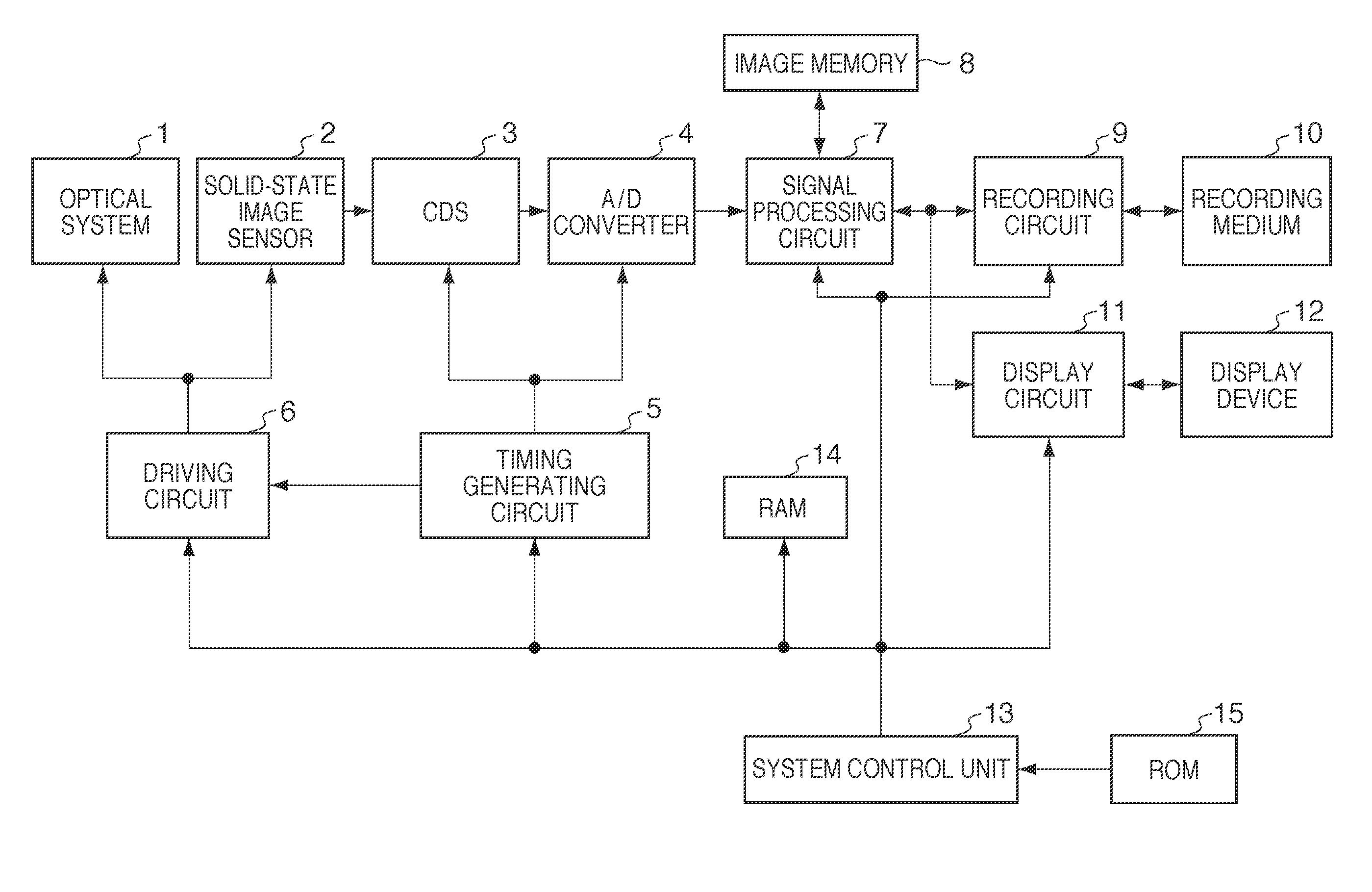
Image

Examples
embodiment 1
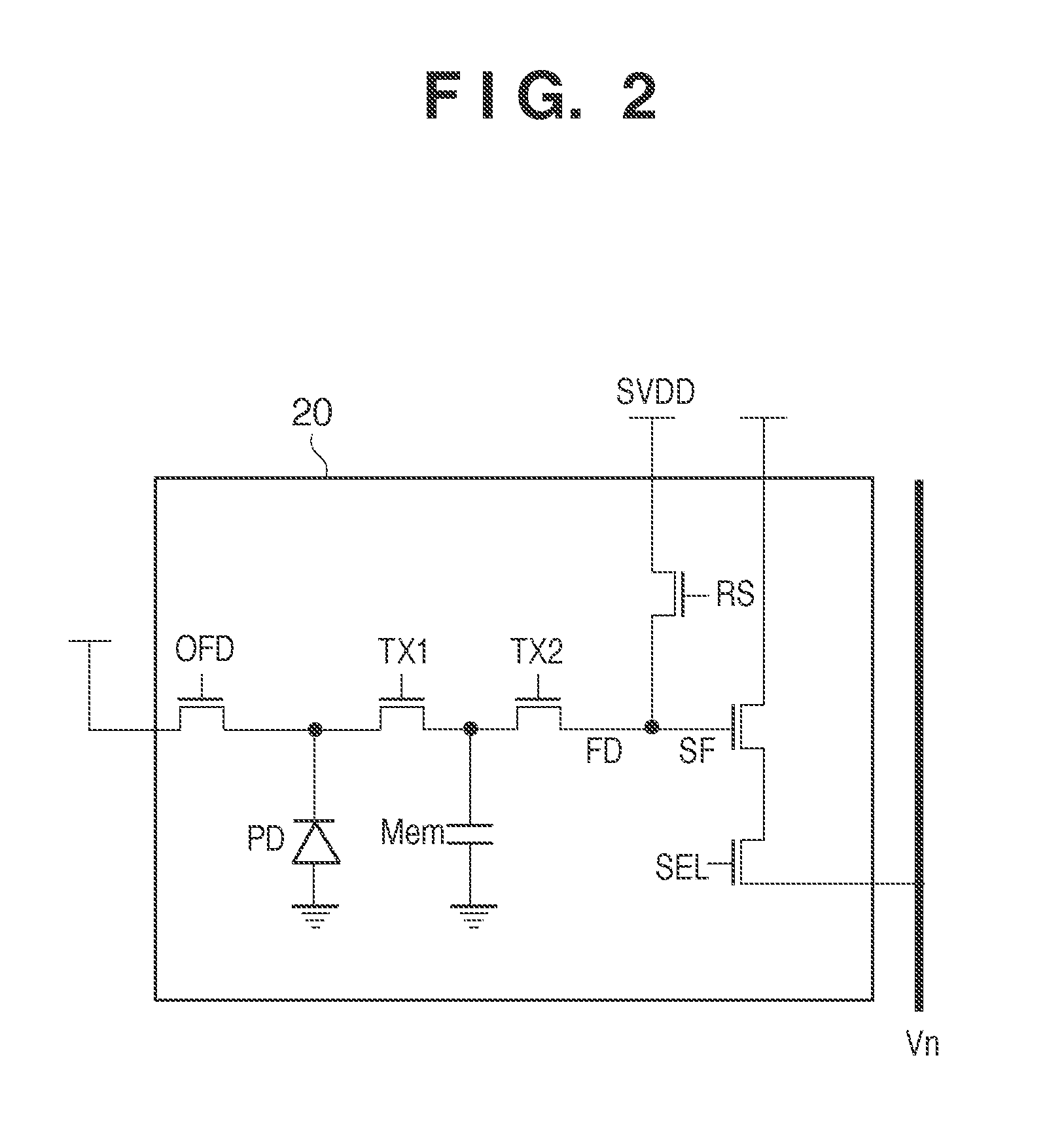
[0026]Below is a description of a driving method for a solid-state image sensor of Embodiment 1 of the present invention with reference to the timing chart in FIG. 3A. In FIG. 3A, transitions between three states called “exposure” (indicated by A), “batch transfer” (indicated by B), and “readout” (indicated by C) are performed in accordance with a vertical synchronization signal. The state called “exposure” is the start of the actual exposure period due to the first polarity change (falling edge) of the OFD control terminal shown in the figure. The state called “batch transfer” is the end of the actual exposure period due to the first polarity change (rising edge) of the first transfer gate TX1 shown in the figure. Changing the polarity of the OFD control terminal and the first transfer gate TX1 at once for all of the pixels in the imaging region enables full-screen simultaneous holding to be performed, and object distortion does not occur in principle. The state called “readout” is...
embodiment 2
[0028]Below is a description of a driving method of Embodiment 2 of the present invention with reference to the timing chart in FIG. 3B and the flowchart in FIG. 4. In Embodiment 1, both maintenance of saturation charge amount and a reduction in the probability of generation of dark current and scratches in the actual exposure period are achieved while keeping a balance therebetween, by changing the electric potential of the first transfer gate TX1 among three electric potentials. Incidentally, in a high ISO sensitivity situation or a low brightness situation in which the saturation charge amount is not very high, or the like, problems such as blocked up highlights (saturation deficit) do not readily occur even when the electric potential is set such that the hole storage state is achieved below the gate electrode of the first transfer gate TX1 in the actual exposure period as well. Embodiment 2 focuses on this property.
[0029]First is a description of a control method shown in FIG. ...
PUM
 Abstract
Description
Claims
Application Information