Layout overlap detection with selective flattening in computer implemented integrated circuit design

a technology of integrated circuit design and overlap detection, applied in computer aided design, program control, instruments, etc., can solve problems such as production yields being negatively impacted, violations, and increase in manufacturing cos

Inactive Publication Date: 2000-01-04
SYNOPSYS INC
View PDF7 Cites 196 Cited by
  • Summary
  • Abstract
  • Description
  • Claims
  • Application Information

AI Technical Summary

Problems solved by technology

Although design rule violations may not necessarily result in a non-functional integrated circuit, production yields may be negatively impacted with a corresponding increase in the cost of manufacture or other circuit problems can result.
Violations occur where this mapping is faulty.
However, even under this approach, each time an integrated circuit design is modified, it needs to be re-run through DRC and LVS checking procedures.
However, performing DRC and LVS checking on a densely populated circuit (as performed by flat DRC programs) is memory and input / output (I / O) intensive and relatively inefficient in terms of computer processing time since each instance of a cell must be checked for conformity with the layout verification rules.
In fact, layout verification programs can often take many hours to perform on high density integrated circuits.
One problem with DRC and LVS checkers arises when the processes encounter juxtaposed cells.
But merely prohibiting overlap of cells is not acceptable since circuit design requires that cells overlap to create, for example, full width conductors, inputs and outputs to the cell or to reduce the size of routing resources.
However, this method is inefficient since new must be cells created and design rule checks performed on each of the new cells.
Further, it is not desirable to build and store inverse layout trees each time the circuit is modified.
Further still, it is not desirable to expend time or system resources in building large intermediate data structures.
Further, the above-described DRC and LVS checking processes are lengthy to perform and must be performed each time the design of the circuit is modified, even if the modification is relatively minor or isolated.
Clearly, the prior art processes are inefficient particularly when DRC and LVS processes must be re-run on moderately or only slightly modified layout database information.

Method used


Image

  • Layout overlap detection with selective flattening in computer implemented integrated circuit design
  • Layout overlap detection with selective flattening in computer implemented integrated circuit design
  • Layout overlap detection with selective flattening in computer implemented integrated circuit design

Examples


Embodiment Construction

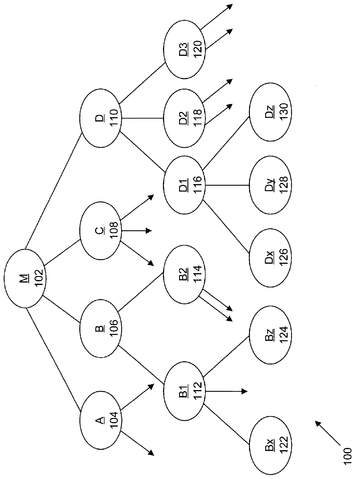
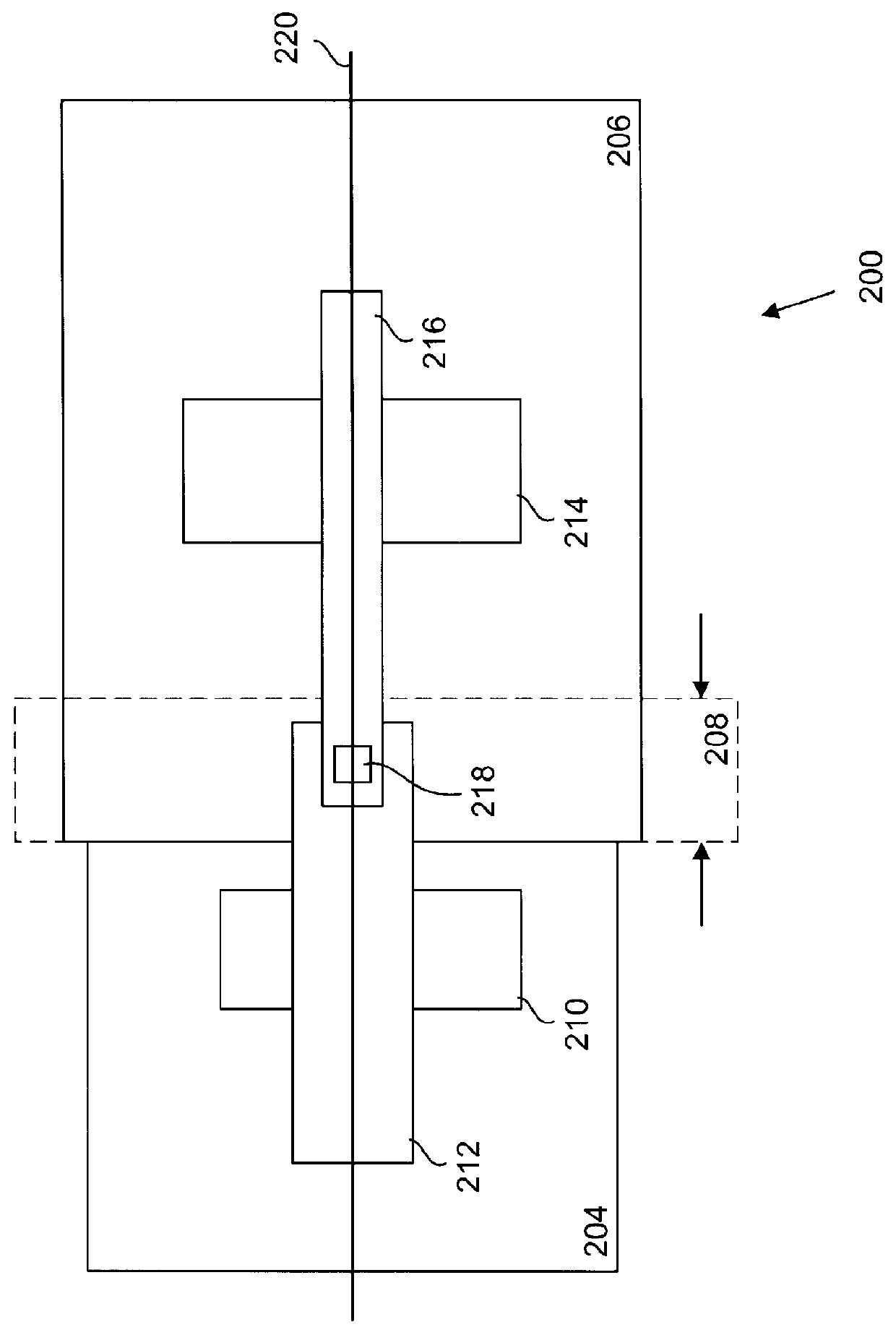
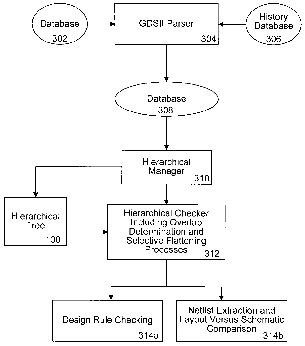
In the following description of the preferred embodiment, reference is made to the accompanying drawings which form a part hereof, and in which is shown by way of illustration a specific embodiment in which the invention may be practiced. It is to be understood that other embodiments may be utilized and that changes may be made without departing from the scope of the present invention. For purposes of illustration the following description describes the present invention as used in the design of CMOS integrated circuits. It is contemplated, however, that the present invention can be used in the design and manufacture of bi-polar or SOS integrated circuits or integrated circuits manufactured using any other semiconductor process. It is further contemplated that the method of the present will be carried out using a computer system having a CPU, memory, secondary storage devices, displays and human interface means, a workstation or a similar machine capable of manipulating symbolic log...


PUM


Abstract

The present invention relates to a method for efficiently performing hierarchical design rules checks (DRC) and layout versus schematic comparison (LVS) on layout areas of an integrated circuit where cells overlap or where a cell and local geometry overlap. With the present invention, a hierarchical tree describes the integrated circuit's layout data including cells having parent-child relationships and including local geometry. The present invention performs efficient layout verification by performing LVS and DRC checking on the new portions of an integrated circuit design and layout areas containing overlapping cells. When instances of cells overlap, the present invention determines the overlap area using predefined data structures that divide each cell into an array of spatial bins. Each bin of a parent is examined to determine if two or more cell instances reside therein or if a cell instance and local geometry reside therein. Once overlap is detected, the areas of the layout data corresponding to the overlap areas are selectively flattened prior to proceeding to DRC and LVS processing. During selective flattening of the overlap areas, the hierarchical tree is traversed from the top cell down through intermediate nodes to the leaf nodes. Each time geometry data is located during the traversal, it is pushes directly to the top cell without being stored in intermediate locations. This provides an effective mechanism for selective flattening.

Description

1. Field of the InventionThe present invention relates to layout verification for an integrated circuit device. More particularly, the present invention relates to a method for improving the process of design rule and layout versus schematic verification for integrated circuit devices.2. Prior ArtIn the design of an integrated circuit, a designer develops a high level language (e.g., VHDL) design and converts this into a netlist using circuit synthesis or logic capture computer implemented programs. The netlist represents logic elements and their interconnections that perform the desired circuit functions outlined in the high level circuit design. Using the netlist, a circuit layout is developed that translates the electrical symbols and connections into primitive geometric patterns ("primitives or geometry") from which transistors or other logic elements are formed and which are to be etched onto the semiconductor device.The various primitives specify various geometric objects such...

Claims


Application Information

Patent Timeline
Patent Type & Authority Patents(United States)
IPC IPC(8): G06F17/50
CPCG06F17/5081G06F30/398
Inventor HO, WAI-YANTANG, HONGBO
Owner SYNOPSYS INC
Why Eureka
Try Eureka