Method for measuring epitaxial film thickness of multilayer epitaxial wafer
a multi-layer epitaxial wafer and epitaxial film technology, applied in the direction of optical radiation measurement, semiconductor/solid-state device testing/measurement, instruments, etc., can solve the problems of difficult film thickness measurement, complicated interference pattern thus obtained, and destructive measurement of conventional measuremen
- Summary
- Abstract
- Description
- Claims
- Application Information
AI Technical Summary
Problems solved by technology
Method used
Image
Examples
embodiment 1
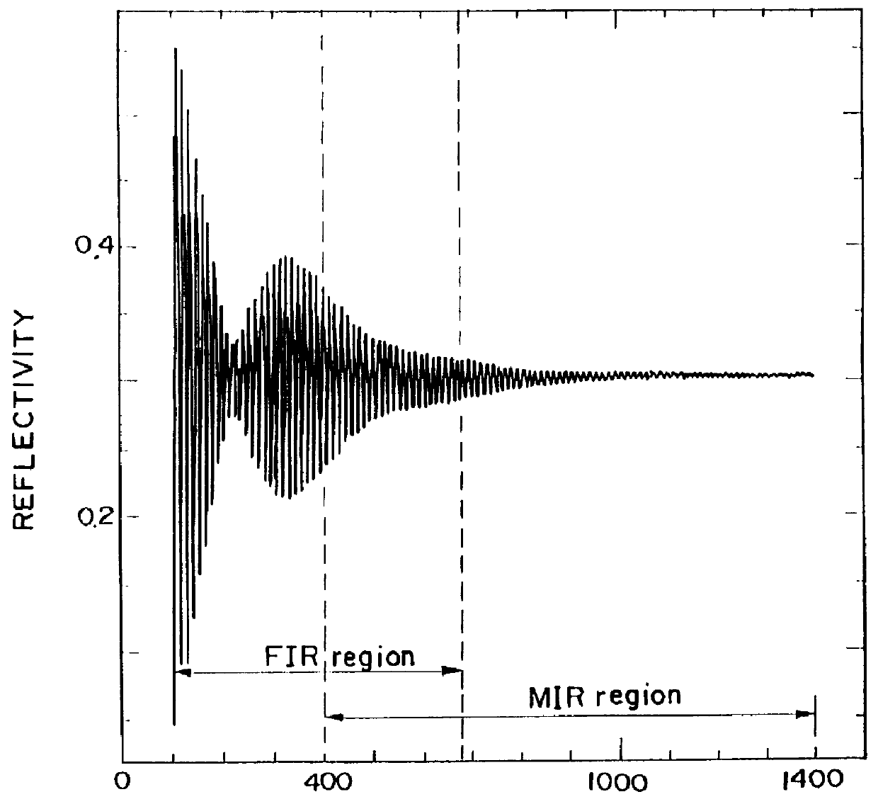
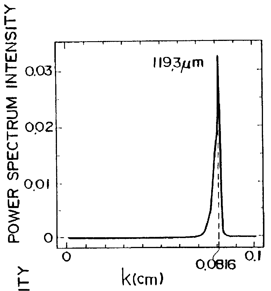
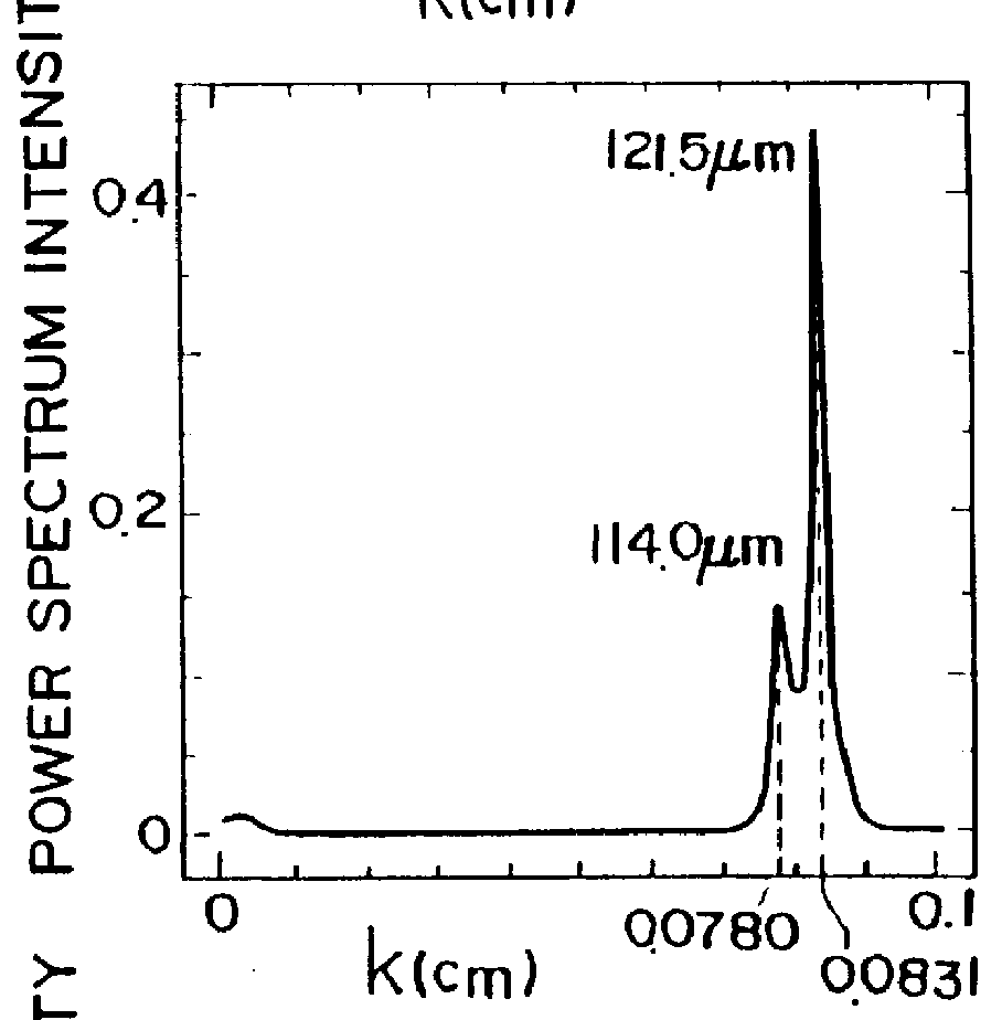
Each of eight kinds of two-layer structure epitaxial wafers (n.sup.- / n.sup.+ / p.sup.++ structure, dopant: P.sup.- / P.sup.+ / B.sup.++) was formed on a single crystalline silicon substrate of 10 to 20 m.OMEGA.cm in specific resistance by the conventional epitaxial method so that target values for the film thickness (Tvg) and the specific resistance (.rho.) shown in table 1 were obtained. The reflection spectrum in the middle infrared and far infrared regions was measured for each epitaxial wafer thus obtained. Further, the value of spreading resistance (hereinafter referred to as "SR") of the oblique polished surface was measured.
The reflection spectrum in the middle infrared region and in the far infrared region were measured. That is, in the middle infrared (MIR) 1400 to 400 cm.sup.-1 region, the measurement was performed under the following condition (light source: SiC, beam splitter: Ge / KBr, detector: DTGS (Deuterated Triglycine Sulfate)(CsI) window plate), in the 680 to 105 cm.su...
embodiment 2
In the same manner as the embodiment 1, each of four kinds of two-layer structure epitaxial wafers (n.sup.- / n.sup.+ / p.sup.++ structure, dopant: P.sup.- / P.sup.+ / B.sup.++) was formed on a single crystalline silicon substrate of 10 to 20 m.OMEGA.cm in specific resistance by the conventional epitaxial method so that target values for the film thickness (Tvg) and the specific resistance (.rho.) shown in Table 4 were obtained. The specific resistance of the first layers of all the wafers was set to about 50 m.OMEGA.cm. The reflection spectrum in the far infrared region of 479 to 50 cm.sup.-1 was measured for each epitaxial wafer thus obtained under the condition: light source: SiC, beam splitter: Mylar polyester film (6 .mu.m in thickness), detector: DTGS (PE window plate)). FIGS. 12A to FIG. 15B show the far infrared reflection spectra of the two-layer epitaxial wafers of the four kinds of samples (FIGS. 12A, 13A, 14A, 15A) and the MEM-analyzed spectra thereof (FIGS. 12B, 13B, 14B, 1...
PUM
 Abstract
Description
Claims
Application Information


