Method of making a high density multilayer wiring board

a multi-layer, wiring board technology, applied in the manufacture of final products, semiconductor/solid-state device details, non-metallic protective coating applications, etc., can solve the problems of not yet gaining wide acceptance by pcb makers, occupying valuable space on the board, and high cost of build-up boards

Inactive Publication Date: 2000-02-22
ANG TECH
View PDF10 Cites 54 Cited by
  • Summary
  • Abstract
  • Description
  • Claims
  • Application Information

AI Technical Summary

Problems solved by technology

However, in a conventional printed wiring board, these vias use up valuable space on the board.
The cost associated with build-up boards is quite high and has not yet gained wide acceptance by PCB makers.
As was noted above, a difficulty in providing compact multilayer printed wiring boards for I/O intensive, chip-size packages is that the input/output connections of these packages are typically arrayed in the form of a two-dimensional matrix and have extremely fine pitches....

Method used


Image

  • Method of making a high density multilayer wiring board
  • Method of making a high density multilayer wiring board
  • Method of making a high density multilayer wiring board

Examples


Embodiment Construction

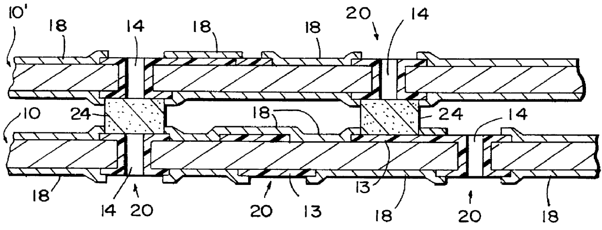
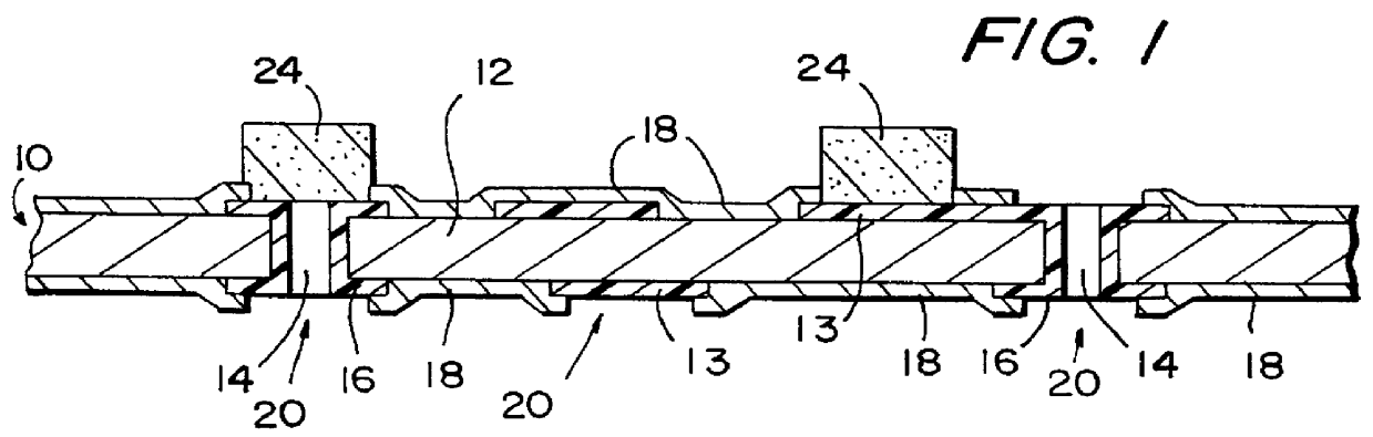
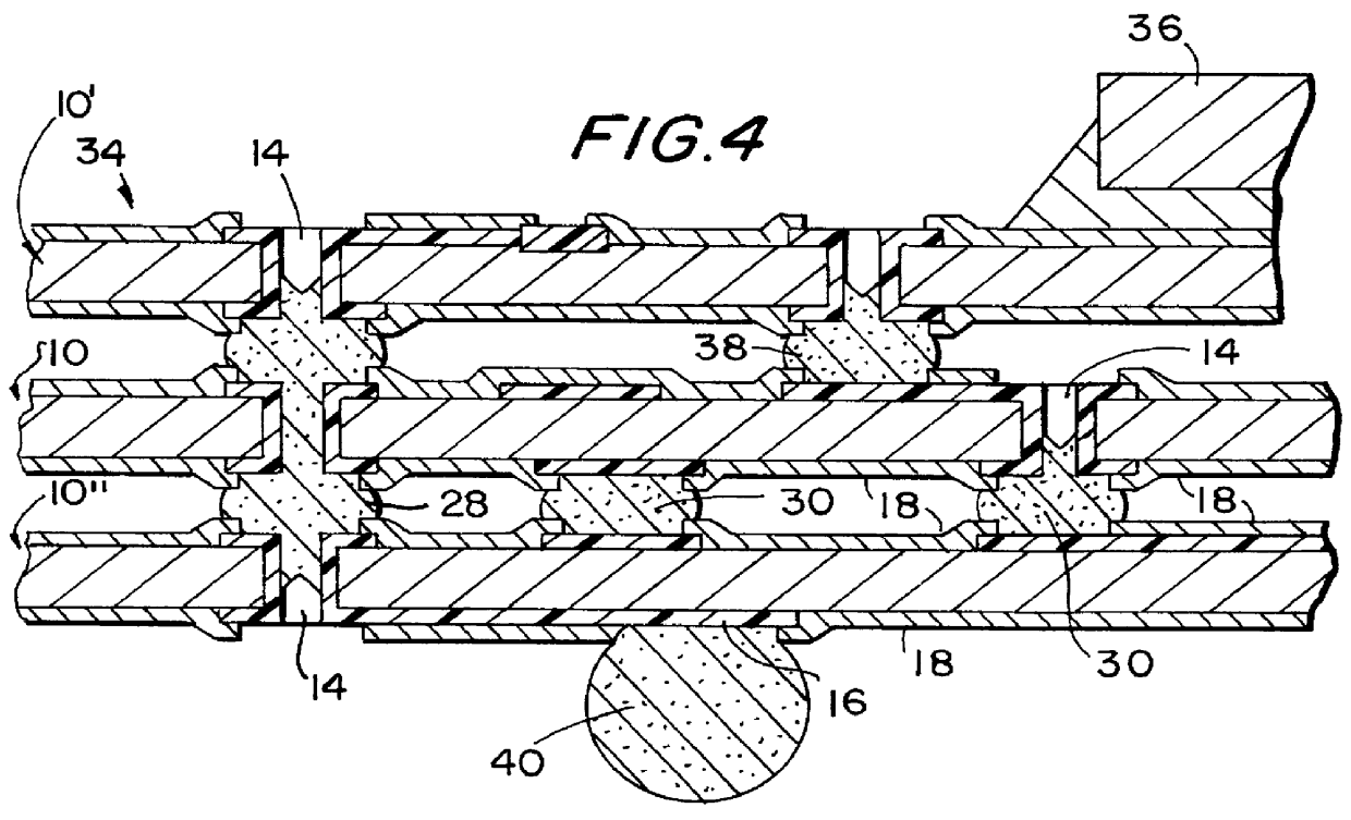
Referring now to the drawings in detail, and especially to FIG. 1, in accordance with a preferred embodiment of the present inventive process, there is initially provided a double-sided board 10 including a substrate 12 made of a dielectric material such as, for example, an epoxy-resin (e.g. FR-4). The substrate 12 may also be made of polyimide or Bismaleimide Triazene ("BT") resin although other materials having similar dielectric properties may be employed. Deposited on the top and / or bottom surface of the substrate 12 is a patterned conductive layer 13 such as, for example, a signal, power or ground plane. The conductive layer 13 may be deposited by, for example, printing or etching and made from any conductive material such as, for example, copper or aluminum.

The substrate 12 may have a plurality of via holes 14 defined through the thickness of the substrate 12. The via holes 14 may be formed by mechanical drilling. Advantageously, smaller via hole diameters than those of the ...


PUM

PropertyMeasurementUnit
Temperatureaaaaaaaaaa
Dielectric polarization enthalpyaaaaaaaaaa
Densityaaaaaaaaaa

Abstract

A process of making a multilayer printed wiring board assembly. The process includes the steps of providing a first and a second substrate made of a dielectric material; depositing a first wiring pattern on the first substrate and a second wiring pattern on the second substrate with a conductive material; depositing a dielectric material on the first and second wiring patterns and defining a via connecting zone on the first and the second wiring pattern for communicating signals between the first and the second wiring pattern by exposing a selective portion of the first and second wiring patterns; depositing a conductive bonding material on the via connecting zone of one of the first and the second wiring pattern; arranging the first and the second substrate in sandwiched juxtaposition such that the via connecting zones of the first and the second wiring pattern are opposite each other and in substantial alignment with each other so that the conductive bonding material deposited on the one of the via connecting zones contacts another one of the via connecting zones; and curing the deposited bonding material thereby forming a conductive joint connecting the first and the second via connecting zones.

Description

1. Field of the InventionThe present invention relates to methods of making printed wiring boards and more particularly, to a method of making high density multilayer wiring boards by affixing a plurality of double-sided boards through inter-layer conductive paths or vias.2. Description of the Related ArtThe demand for greater miniaturization of electronic products such as notebook computers, cellular phones, camcorders and the like has presented new challenges for printed circuit board (PCB) makers as more and more high density integrated circuit (IC) chip packages such as ball grid arrays (BGAs) and chip-size packages (CSPs) become more readily available. These chip packages, which contain high-density integrated circuits therewithin, typically have an extremely high number of input / output (I / O) connections. To provide greater surface area for the I / O connections while minimizing the footprint of the packages, these chip packages typically have 2-dimensional arrays of solder bumps...

Claims


Application Information

Patent Timeline
IPC IPC(8): H05K3/34H05K3/36H05K3/46H05K3/28H05K1/14
CPCH05K3/3436H05K3/368H05K3/462H05K1/144Y10T29/49128H05K3/284H05K3/3484H05K2201/0195H05K2201/09536H05K2201/096H05K2201/10666H05K2201/10977H05K2203/1327Y10T29/49165Y10T29/49126Y10T29/49144H05K3/28H05K3/3485Y02P70/50
Inventor WANG, PETERHUANG, YU-WEN
Owner ANG TECH
Why Eureka
Try Eureka