Plug or via formation using novel slurries for chemical mechanical polishing

a technology of mechanical polishing and slurries, which is applied in the direction of polishing compositions, other chemical processes, chemistry apparatuses and processes, etc., can solve the problems of insufficient tungsten layer manufacturability, voids or open circuit formation, and inability to print high resolution lines

Inactive Publication Date: 2000-04-04
INTEL CORP
View PDF1 Cites 90 Cited by
  • Summary
  • Abstract
  • Description
  • Claims
  • Application Information

AI Technical Summary

Problems solved by technology

Such recessing causes a non-planar via layer to be formed which impairs the ability to print high resolution lines during subsequent photolithography steps and can cause the formation of voids or open circuits in the metal interconnections formed above.
As such, high pH slurries have been found inadequate to manufacturably polish tungsten layers in an integrated circuit.
Unfortunately, however, s

Method used


Image

  • Plug or via formation using novel slurries for chemical mechanical polishing
  • Plug or via formation using novel slurries for chemical mechanical polishing
  • Plug or via formation using novel slurries for chemical mechanical polishing

Examples


Embodiment Construction

Novel slurries for chemical mechanical polishing of thin films used in high density integrated circuits are described. In the following description numerous specific details are set forth, such as specific machinery materials, thicknesses, etc., in order to provide a thorough understanding of the present invention. It will be obvious, however, to one skilled in the art that the present invention may be practiced without these specific details. In other instances, other well-known semiconductor processes and machinery have not been described in particular detail in order to avoid unnecessarily obscuring the present invention.

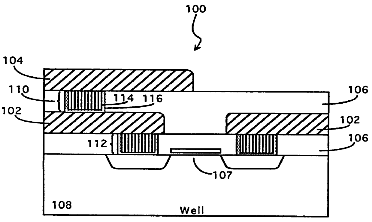
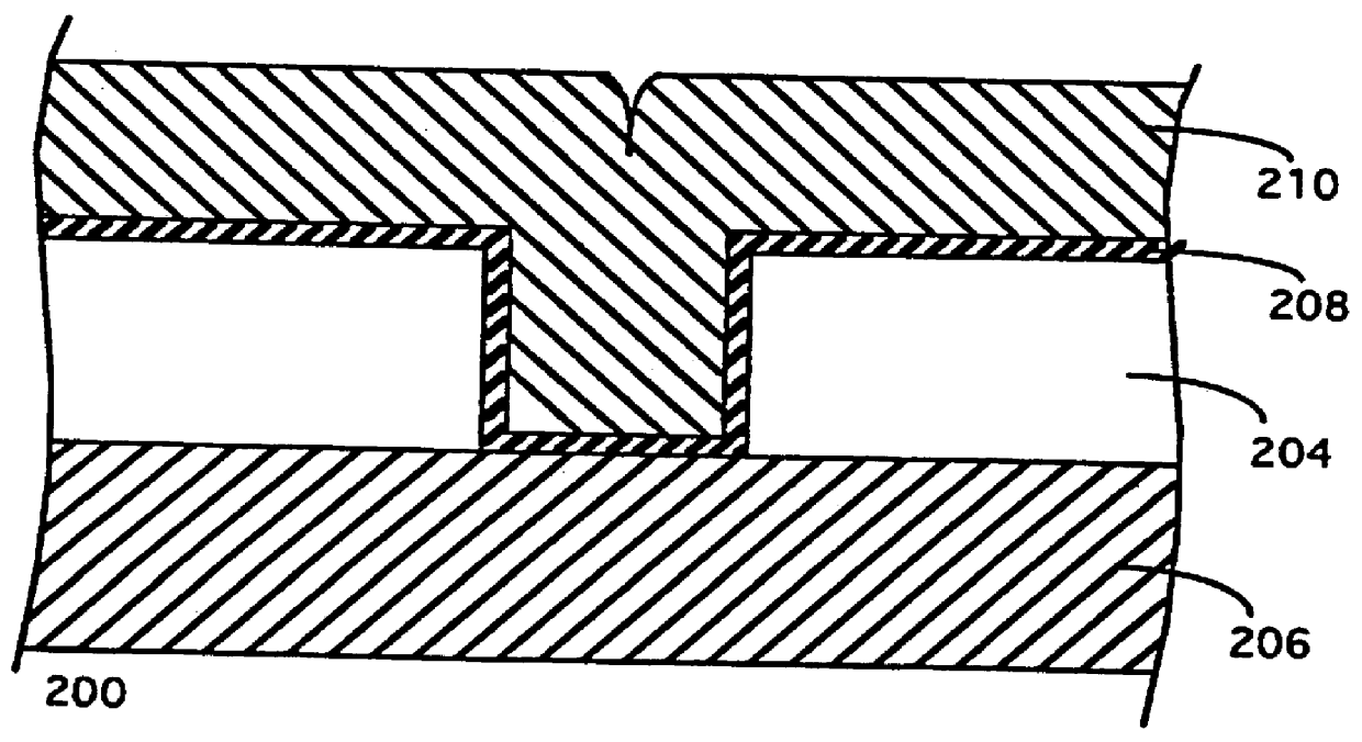
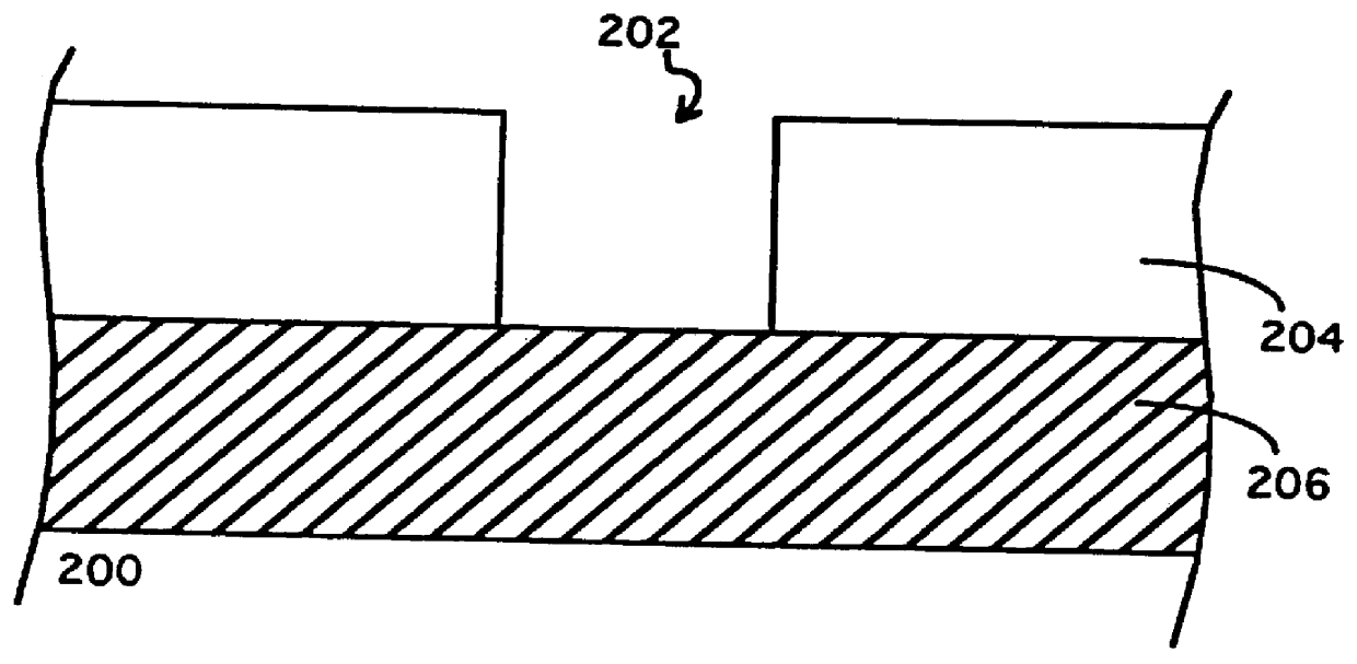
The present invention describes novel slurries for the chemical mechanical polishing (CMP) of thin films used in a semiconductor integrated circuit. The novel slurries and CMP processes of the present invention are preferably used to form a via connection or plug between conductive layers of a semiconductor device. The teachings of the present invention, however,...


PUM


Abstract

Novel slurries for the chemical mechanical polishing of thin films used in integrated circuit manufacturing. A tungsten slurry of the present invention comprises an oxidizing agent, such as potassium ferricyanide, an abrasive such as silica, and has a pH between two and four. The tungsten slurry of the present invention can be used in a chemical mechanical planarization process to polish back a blanket deposited tungsten film to form plugs or vias. The tungsten slurry can also be used to polish copper, tungsten silicide, and titanium nitride. A second slurry, which is a 9:1 dilution of the tungsten slurry is ideal for chemical mechanical polishing of titanium nitride films. A third slurry of the present invention comprises a fluoride salt, an abrasive such as silica and has a pH</=8. The third slurry can be used to polish titanium films.

Description

1. Field of the InventionThe present invention relates to the field of semiconductor integrated circuit manufacturing, and more specifically, to improved slurries for the chemical mechanical polishing (CMP) of thin films used in semiconductor integrated circuit manufacturing.2. Description of Relevant ArtToday, integrated circuits are made up of literally millions of active devices formed in or on a silicon substrate or well. The active devices which are initially isolated from one another are later connected together to form functional circuits and components. The devices are interconnected together through the use of well-known multilevel interconnections. A cross-sectional illustration of a typical multilevel interconnection structure 100 is shown in FIG. 1. Interconnection structures normally have a first layer of metallization, an interconnection layer 102 (typically aluminum alloys with up to 3% copper), a second level of metallization 104, and sometimes a third or even fourth...

Claims


Application Information

Patent Timeline
IPC IPC(8): C09K3/14C09G1/00C09G1/02H01L21/02H01L21/321H01L21/768
CPCC09G1/02C09K3/1463H01L21/76843H01L21/7684H01L21/3212
Inventor CADIEN, KENNETH C.FELLER, DANIEL A.
Owner INTEL CORP
Why Eureka
Try Eureka