Process for removal of undersirable conductive material on a circuitized substrate and resultant circuitized substrate

a technology of circuitized substrates and conductive materials, applied in the field of circuitized substrates, can solve the problems of electrical shorting between the circuit features of the finished circuit pattern, inadequately addressed, and further electrical shorting

Inactive Publication Date: 2000-05-16
META PLATFORMS INC
View PDF9 Cites 11 Cited by
  • Summary
  • Abstract
  • Description
  • Claims
  • Application Information

AI Technical Summary

Problems solved by technology

One of the difficulties not adequately addressed heretofore occurs after the remaining resist has been removed, a residual catalyst layer (e.g., tin and palladium layer) remains between the circuit features (e.g. lines) of the circuit pattern.
Another difficulty is that when the catalyst layer has a circuit pattern deposited thereon, trace amounts of the circuit material (e.g., copper) in the circuit pattern, seep under the resist into the residual catalyst layer which causes further electrical shorting.
If the catalyst layer and residual circuit material are not adequately removed, electrical shorting between the circuit features o

Method used


Image

  • Process for removal of undersirable conductive material on a circuitized substrate and resultant circuitized substrate
  • Process for removal of undersirable conductive material on a circuitized substrate and resultant circuitized substrate
  • Process for removal of undersirable conductive material on a circuitized substrate and resultant circuitized substrate

Examples


Embodiment Construction

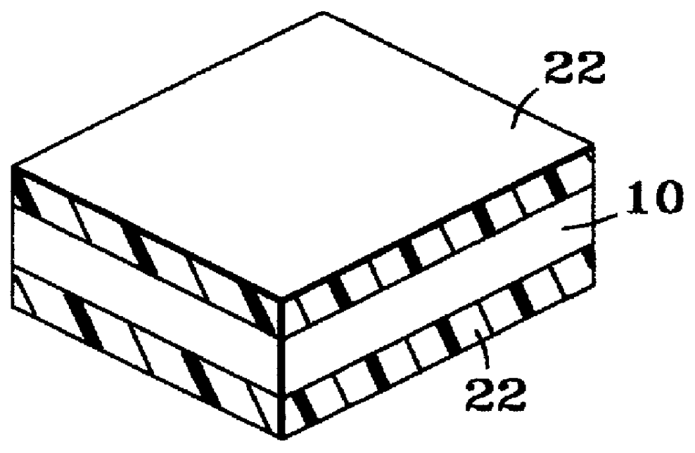
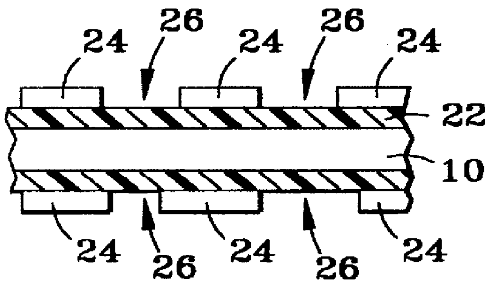
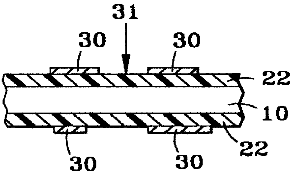
FIGS. 1-8 depict a process for removal of undesirable conductive material on a printed circuit and the resultant printed circuit. The undesirable conductive material is a catalyst material and circuit material that has seeped between the circuit lines under the catalyst material during processing. The undesirable conductive material causes electrical leakage problems if not removed.

FIGS. 1 and 2 show an optional step for preparing a surface of a substrate 10 before coating with a catalyst layer 22. The substrate may be any of a variety of dielectric substrates, including thermoplastic and thermosetting resins, glass and ceramics. Typical thermosetting polymeric materials include epoxy, phenolic base materials, polyimides, and fluoropolymers. The dielectric substrate may be molded from polymeric materials which may or may not include reinforcement. Presently, preferred substrates include epoxies, polyimides, and fluoropolymers. In particular, FIG. 1 depicts a substrate 10 laminated b...


PUM

PropertyMeasurementUnit
Electrical conductoraaaaaaaaaa
Areaaaaaaaaaaa

Abstract

A process for removal of undesirable conductive material (e.g., catalyst material and seeped circuit material) on a circuitized substrate and the resultant circuitized substrates disclosed. Such process and resultant circuit effectively address the electrical shorting problems caused by nonremoval of the residual catalyst material and circuit material which has seeped under the residual catalyst material. The process includes the steps of: a) providing a catalyst layer (e.g., palladium and tin) having circuit pattern (e.g., copper) thereon; b) pretreating the catalyst layer and the circuit pattern (e.g., with a cyanide dip) for removal of undesirable portions of each which cause electrical leakage between circuit lines of the circuit pattern; c) oxidizing the catalyst layer and the circuit pattern (e.g., with chlorite, permanganate, hydrogen peroxide, or air at a temperature elevated above ambient conditions); and d) removing the undesirable portions of the catalyst layer and the undesirable portions of the circuit pattern (e.g., with a cyanide submersion). The resultant circuitized substrate includes a circuit pattern on a catalyst layer wherein undesirable portions of the catalyst layer and circuit pattern are completely removed between the circuit features of the circuit pattern so that electrical leakage between the circuit features does not occur.

Description

1. Field of the InventionThe present invention relates generally to circuitized substrates and more specifically to a process for removal of undesirable conductive material (e.g., a catalyst layer) on a printed circuit and the resultant printed circuit.2. Description of the Related ArtIn the manufacture of printed circuit boards, a conductive circuit pattern is provided on at least one surface of a dielectric substrate. The circuit pattern can be formed on the substrate using a variety of known techniques. One of the better known techniques includes the electroless direct bond (EDB) technique, wherein copper is electrolessly plated directly onto the surface of the substrate in a desired pattern. The circuit pattern may include conductor lines on the surface of the substrate as well as in holes (often referred to as plated through holes) which connect one or more of the conductive layers together. Since the dielectric substrate is non-conductive, it is generally necessary to catalyze...

Claims


Application Information

Patent Timeline
IPC IPC(8): H05K3/26H05K3/18
CPCH05K3/184H05K3/26H05K2201/0761H05K2203/0796Y10T428/12861Y10T428/12868Y10T428/24917Y10T428/12396Y10T428/12715Y10S428/901Y10T428/31678
Inventor ARRINGTON, EDWARD LEECAMP, JOHN CHRISTOPHERDAY, ROBERT JEFFREYFEY, EDMOND OTTOGUNTHER, CURTIS MICHAELMILLER, THOMAS RICHARD
Owner META PLATFORMS INC
Why Eureka
Try Eureka