Semiconductor optical reflector and a method of manufacturing the same

a technology of semiconductor optical reflector and manufacturing method, which is applied in the direction of optical elements, semiconductor lasers, instruments, etc., can solve the problems of difficult and lengthy process of manufacturing such a grating, the inability to manufacture a type of varying-period grating, and the increase of implementation difficulty and time. achieves the effect of high coupling coefficien

Inactive Publication Date: 2000-05-16
OCLARO NORTH AMERICA
View PDF9 Cites 49 Cited by
  • Summary
  • Abstract
  • Description
  • Claims
  • Application Information

AI Technical Summary

Benefits of technology

An object of the present invention therefore consists in finding a solution for making a semiconductor optical reflector that has a wide spectrum band regardless of the value of the coupling coefficient .kappa., so as to avoid the problems posed by forming a grating having a high coupling coefficient.
A solution for making such a reflector has been studied and consists in manufacturing a grating having a continuously varying period .LAMBDA.. That solution appears to be advantageous in theory because such a grating has a wide spectrum window independently of the coupling coefficient. Unfortunately, in practice, manufacturing such a grating is a difficult and lengthy process. That type of varying-period grating cannot be manufactured by implementing a conventional method using holographic interference. Another method used to manufacture that type of grating requires as many etching steps as there are different period values. As a result, the implementation difficulty and time are considerably increased, and the efficiency of the method is considerably decreased.
The present invention makes it possible to mitigate the above-mentioned drawbacks because it provides a semiconductor optical reflector that is made up of a plurality of cascaded Bragg reflector sections and that has a wide spectrum window independent of the value of the coupling coefficient.
This method is very simple and quick to implement because the holographic grating of the stack structure is formed conventionally, without seeking to increase index step or depth, and the cascaded sections are formed in a single etching step.
This holographic method takes a little longer to implement than the preceding method. However, it remains simple to implement and it is easy to control, unlike the method of manufacturing a grating having a continuously varying period.

Problems solved by technology

Unfortunately, in practice, manufacturing such a grating is a difficult and lengthy process.
That type of varying-period grating cannot be manufactured by implementing a conventional method using holographic interference.
As a result, the implementation difficulty and time are considerably increased, and the efficiency of the method is considerably decreased.

Method used


Image

  • Semiconductor optical reflector and a method of manufacturing the same
  • Semiconductor optical reflector and a method of manufacturing the same
  • Semiconductor optical reflector and a method of manufacturing the same

Examples


first embodiment

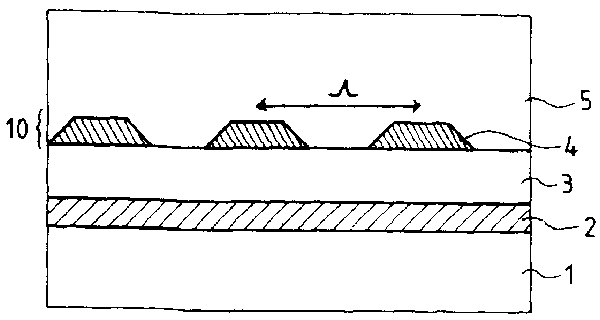
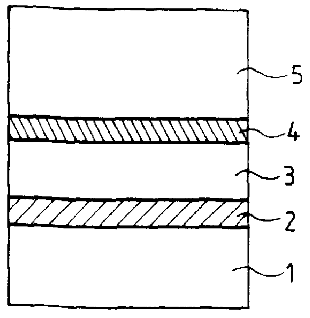
FIG. 4A is a diagrammatic plan view of an optical reflector of the invention. In the example shown, the reflector is made up of two cascaded holographic Bragg grating sections S.sub.1, S.sub.2. Naturally, the invention is not limited to this example, and the reflector may be made up of more than two sections.

In this example, the two sections S.sub.1 and S.sub.2 have identical grating periods .LAMBDA..sub.1 and .LAMBDA..sub.2 and identical lengths L.sub.1 and L.sub.2, but they have different widths W.sub.1 and W.sub.2. As a result of this difference between the widths W of the two sections S.sub.1 and S.sub.2, the proportion of air varies on either side of each section. This variation in the proportion of air from one section to the other causes the effective refractive index n.sub.1, n.sub.2 to vary from one of the two sections S.sub.1 and S.sub.2 to the other, i.e. the mean guiding index of the medium encountered by a light wave varies from one section to the other.
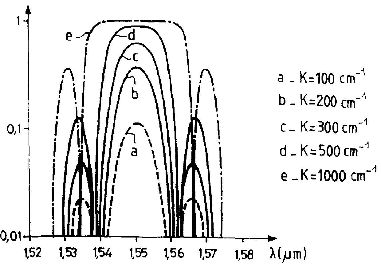
The curve shown ...

second embodiment

FIG. 5 is a diagrammatic plan view of an optical reflector of the invention. In this embodiment, the cascaded holographic Bragg grating sections S.sub.1 and S.sub.2 have the same length L, the same, width W, and therefore the same effective refractive index. However, the period .LAMBDA..sub.1, .LAMBDA..sub.2 of each section S.sub.1, S.sub.2 is different.

The method of manufacturing the reflector consists firstly in forming a stack structure including a top layer of a ternary material or of a quaternary material serving to be etched to form a holographic grating. The top layer is then etched over a first section S.sub.1 of length L to form a crenelated pattern having a given period .LAMBDA..sub.1. The top layer is then etched over another section S.sub.2 that is adjacent to the preceding section and that is of the same length L, to form another crenelated pattern having some other period .LAMBDA..sub.2. Etching the crenelated notches is thus repeated over each section S.sub.i of the r...


PUM


Abstract

The invention relates to a semiconductor optical reflector serving in particular for being disposed facing an integrated laser cavity so as to feed light back into said cavity, and enable it to oscillate continuously. The reflector is made up of a plurality of cascaded Bragg reflector sections. More particularly, said sections are of the same length L and have the same coupling coefficient, and the length L of each pair of sections is given by the following relationship:L= lambda 2 / [(ni+1+ni)x1.7(ni+1 LAMBDA i+1-ni LAMBDA i)]where lambda is the mean value of the Bragg wavelengths reflected by the reflector; ni+1 and ni are the respective effective refractive indices of said adjacent sections; and LAMBDA i+1 and LAMBDA i are the respective periods of said adjacent sections. The reflector of the invention has a wide spectrum band independent of the value of the coupling coefficient.

Description

The present invention relates to a semiconductor optical reflector and to a method of manufacturing such a reflector. It relates more particularly to an optical reflector comprising a plurality of cascaded Bragg reflector sections.Bragg reflectors make it possible to reflect a portion of the light that they receive. They are commonly used in the field of optical transmission. They can be disposed facing an integrated laser cavity so as to return energy to thereto and so as to enable it to oscillate continuously. In which case, they replace the cleaved-face mirrors of non-integrated semiconductor lasers.A Bragg reflector is more particularly defined by a periodic grating made up of two materials having different refractive indices. The reflection ratio of such a device depends both on the difference between the indices of the two component materials, and also on the geometrical shape of the grating. It is proportional to the product of .kappa. multiplied by L, where L is the length o...

Claims


Application Information

Patent Timeline
Patent Type & Authority Patents(United States)
IPC IPC(8): G02B6/124G02B6/12H01S5/12H01S5/183H01S5/00G02B5/08G02B6/122H01S5/14
CPCG02B6/12007G02B6/124H01S5/18361H01S5/1215
Inventor BISSESSUR, HANSGRAVER, CATHERINE
Owner OCLARO NORTH AMERICA
Why Eureka
Try Eureka