

Method for production of dislocation-free silicon single crystal
a technology of silicon single crystal and dislocation-free silicon, which is applied in the direction of crystal growth process, polycrystalline material growth, and protective fluid, etc., can solve the problems of seed crystals developing dislocations, difficult removal of dislocations, and ineffective standard p.sup.- -type crystals or n-type crystals
- Summary
- Abstract
- Description
- Claims
- Application Information
AI Technical Summary
Problems solved by technology
Method used
Image

Examples
example 1
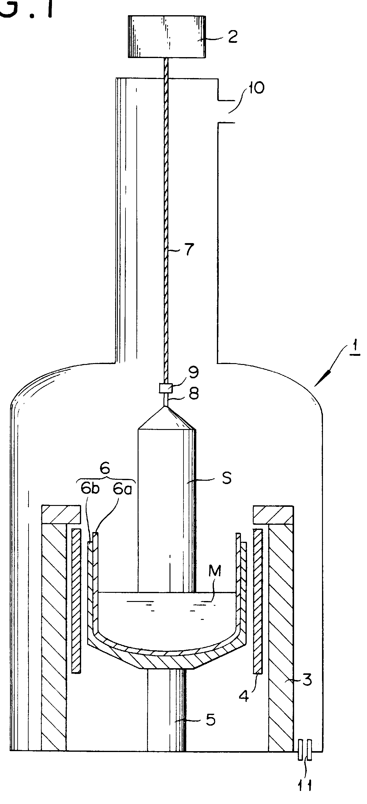
In the apparatus of FIG. 1, a seed crystal was immersed in the melt under the following conditions.
Presence or absence of dislocation in seed crystal: absent
Maximum value of temperature gradient occurring in seed crystal: 9.degree. C. / mm
Immersing rate into melt: 4.0 mm / min
Shape of leading end of seed crystal: flat
Rmax value of part of seed crystal (reference length 0.1 mm) immersed in melt: 30 .mu.m
Surface condition of part of seed crystal immersed in melt: as ground
Dopant concentration in seed crystal: boron=1.times.10.sup.15 cm.sup.-3
Horizontal maximum length of part of seed crystal being immersed in melt at time of completion of immersion: 10 mm
After the immersion of the seed crystal was completed and the crystal was fully wetted with the melt, the main body part of silicon single crystal was grown with no recourse to the Dash's neck.
The silicon single crystal grown under these conditions had the following quality.
Type of conduction: p-type. Crystal diameter: 310 mm (12 inches), ...
example 2
In the apparatus of FIG. 1, a seed crystal was immersed in the melt under the following conditions.
Presence or absence of dislocation in seed crystal: absent
Maximum value of the temperature gradient occurring in seed crystal: 8.degree. C. / mm
Immersing rate into melt: 2.6 mm / min
Shape of leading end of seed crystal: flat
Rmax values of part of seed crystal (reference length 0.1 mm) immersed in melt: 28 .mu.m
Surface condition of part of seed crystal immersed in melt: as ground
Dopant concentration in seed crystal: phosphorus=2.times.10.sup.15 cm.sup.-3
Horizontal maximum length of part of seed crystal being immersed in melt at time of completion of immersion: 15 mm
After the immersion of the seed crystal was completed and the crystal was fully wetted with the melt, the main body part of silicon single crystal was grown with no recourse to the Dash's neck.
The silicon single crystal grown under these conditions had the following quality.
example 3
In the apparatus of FIG. 1, a seed crystal was immersed in the melt under the following conditions.
Presence or absence of dislocation in seed crystal: absent
Maximum value of temperature gradient occurring in seed crystal: 7.degree. C. / mm
Immersing rate into melt: 3.6 mm / min
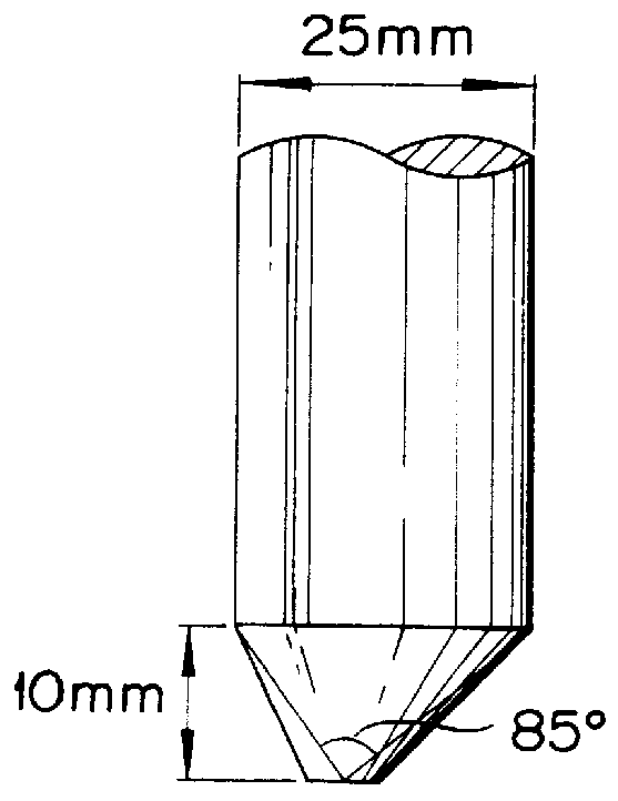
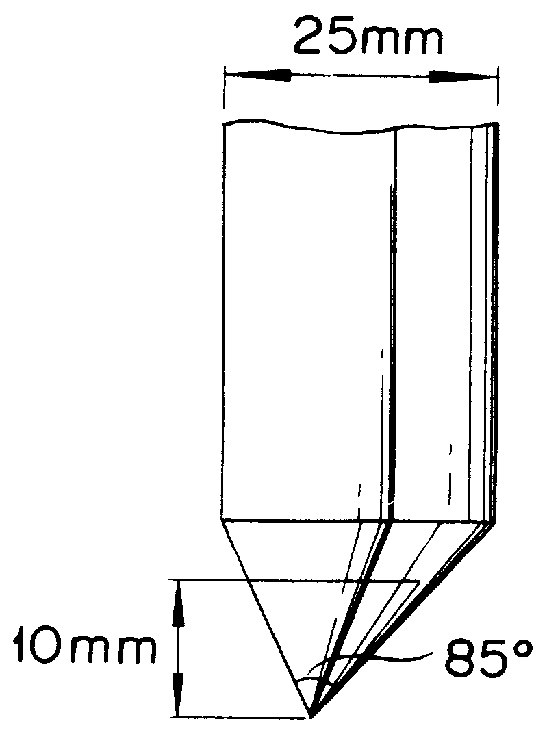
Shape of leading end of seed crystal: convexed downward (as illustrated in FIGS. 2A and 2B)
Angle of leading end / 10 mm of seed crystal: 120 degrees
Rmax value of part of seed crystal (reference length 0.1 mm) immersed in melt: 42 .mu.m
Surface condition of part of seed crystal immersed in melt: as ground
Dopant concentration in seed crystal: phosphorus=2.times.10.sup.14 cm.sup.-3
Horizontal maximum length of part of seed crystal being immersed in melt at time of completion of immersion: 30 mm
After the immersion of the seed crystal was completed and the crystal was fully wetted with the melt, the main body part of silicon single crystal was grown with no recourse to the Dash's neck.
The silicon single crystal grown under ...
PUM
| Property | Measurement | Unit |
|---|---|---|
| length | aaaaa | aaaaa |
| length | aaaaa | aaaaa |
| length | aaaaa | aaaaa |
Abstract
Description
Claims
Application Information