Method of making an organic thin film transistor

a thin film transistor and organic technology, applied in the field of organic thin film transistors, can solve the problems of unsatisfactory material limit the utility of such a process for fabricating low-cost thin film devices, and material unsatisfactory for use in thin film devices

Inactive Publication Date: 2000-08-22
BELL SEMICON LLC +2
View PDF3 Cites 419 Cited by
  • Summary
  • Abstract
  • Description
  • Claims
  • Application Information

AI Technical Summary

Problems solved by technology

The organic polymer formed using such electrochemical polymerization is a polythiophene compound having a carrier mobility of about 10.sup.-5 cm.sup.2 / Vs, which makes this material unsatisfactory for use in thin film FETs.
The organic polymer formed is a poly (3-hexylthiophene) film having a carrier mobility of about 10.sup.-5 cm.sup.2 / Vs to 10.sup.-4 cm.sup.2 / Vs, which makes this material unsatisfactory for use in thin film devices.
However, the process described in Garnier et al. requires the use of expensive evaporation tools, so as to limit the utility of such a process for fabricating low-cost thin film FETs.

Method used


Image

  • Method of making an organic thin film transistor
  • Method of making an organic thin film transistor
  • Method of making an organic thin film transistor

Examples


Embodiment Construction

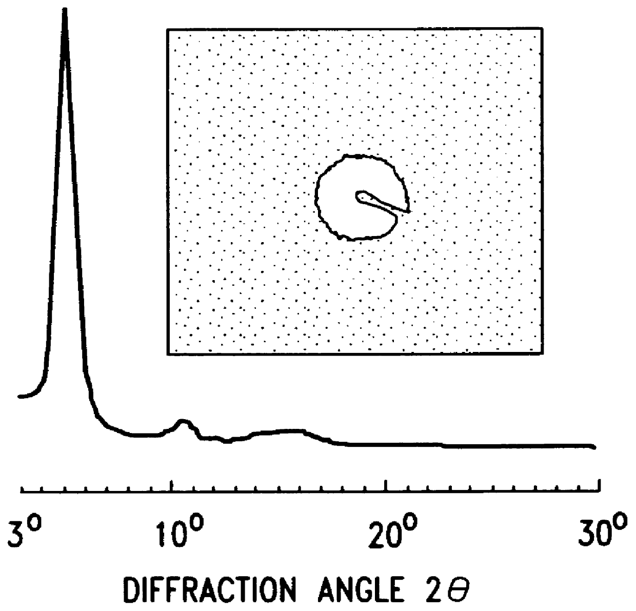
Regioregular poly (3-hexylthiophene) (PHT), poly (3-octylthiophene) (POT) and poly (3-dodecylthiophene) (PDT) were obtained from Aldrich Chemical Company. The linkages in these polymers were at least 98.5% head-to-tail (HT). The polymers had a number averaged molecular weight above 25,000 and polydispersity of about 1.5. These polymers were purified by dissolving them in toluene and precipitating from acetone. The purification was performed three times total and the polymer was then extracted with acetone.

Each regioregular poly (3-alkylthiophene) (0.01 g / ml) was dissolved in chloroform at room temperature and filtered through a 0.200 .mu.m pore size polytetraflouroethylene (PTFE) membrane syringe filter.

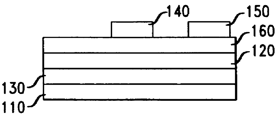
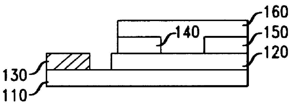
Devices were formed using the above identified regioregular poly (3-alkylthiophene) compounds as the active layer, as generally described above with reference to FIG. 3. The solution containing the dissolved polymer was applied over the insulating layer by casting, with the thickness...


PUM

PropertyMeasurementUnit
concentrationaaaaaaaaaa
conductivityaaaaaaaaaa

Abstract

A process for fabricating thin film transistors in which the active layer is an organic semiconducting material with a carrier mobility greater than 10-3 cm2 / Vs and a conductivity less than about 10-6 S / cm at 20 DEG C. is disclosed. The organic semiconducting material is a regioregular (3-alkylthiophene) polymer. The organic semiconducting films are formed by applying a solution of the regioregular polymer and a solvent over the substrate. The poly (3-alkylthiophene) films have a preferred orientation in which the thiophene chains has a planar stacking so the polymer backbone is generally parallel to the substrate surface.

Description

The present invention relates generally to thin film transistors (TFTs) incorporating an active layer of organic material, and to methods for making such transistors.DESCRIPTION OF THE RELATED ARTRecently, organic materials have been investigated for use as the active semiconductor layer in thin film field effect transistors (FETs). Organic materials are attractive for use as the active semiconductor layer in thin film devices because they are easily processable and are compatible with the plastic substrates on which thin film FETs are typically formed. Such advantages are important when fabricating low-cost, large area devices. In order for an organic material to be useful as the active semiconductor layer in thin film FETs, the resulting devices must have an acceptable on / off ratio. Typically, thin film FETs must have an on / off ratio of at least 10.sup.3. The term on / off ratio as used in this disclosure refers to the ratio of the source-drain current when the transistor is on to t...

Claims


Application Information

Patent Timeline
Patent Type & Authority Patents(United States)
IPC IPC(8): H01L51/05H01L51/30H01L51/40C09K3/00H01L21/336H01L29/786H01L51/00
CPCH01L51/0036H01L51/0003H01L51/0516H01L51/0545H10K71/12H10K85/113H10K10/468H10K10/466
Inventor BAO, ZHENANDODABALAPUR, ANANTHFENG, YIRAJU, VENKATARAM REDDY
Owner BELL SEMICON LLC
Why Eureka
Try Eureka