

Hybrid SOI/bulk semiconductor transistors
a soi/bulk semiconductor transistor, hybrid technology, applied in the direction of transistors, semiconductor devices, electrical equipment, etc., can solve the problems of floating body effect, difficult to maintain transistor electrical characteristics, and increased resistance that is difficult to redu
- Summary
- Abstract
- Description
- Claims
- Application Information
AI Technical Summary
Benefits of technology
Problems solved by technology
Method used
Image

Examples
first embodiment
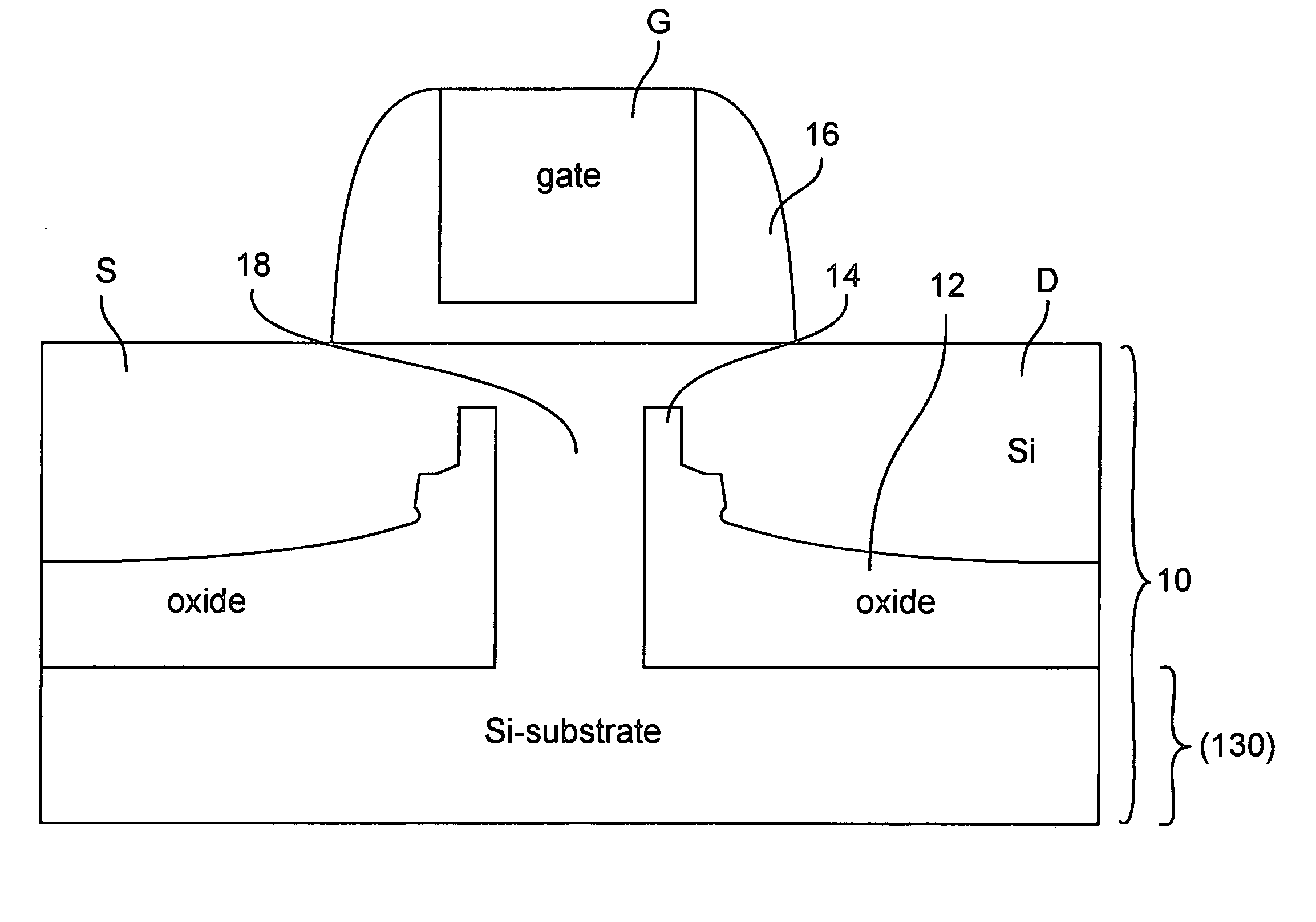
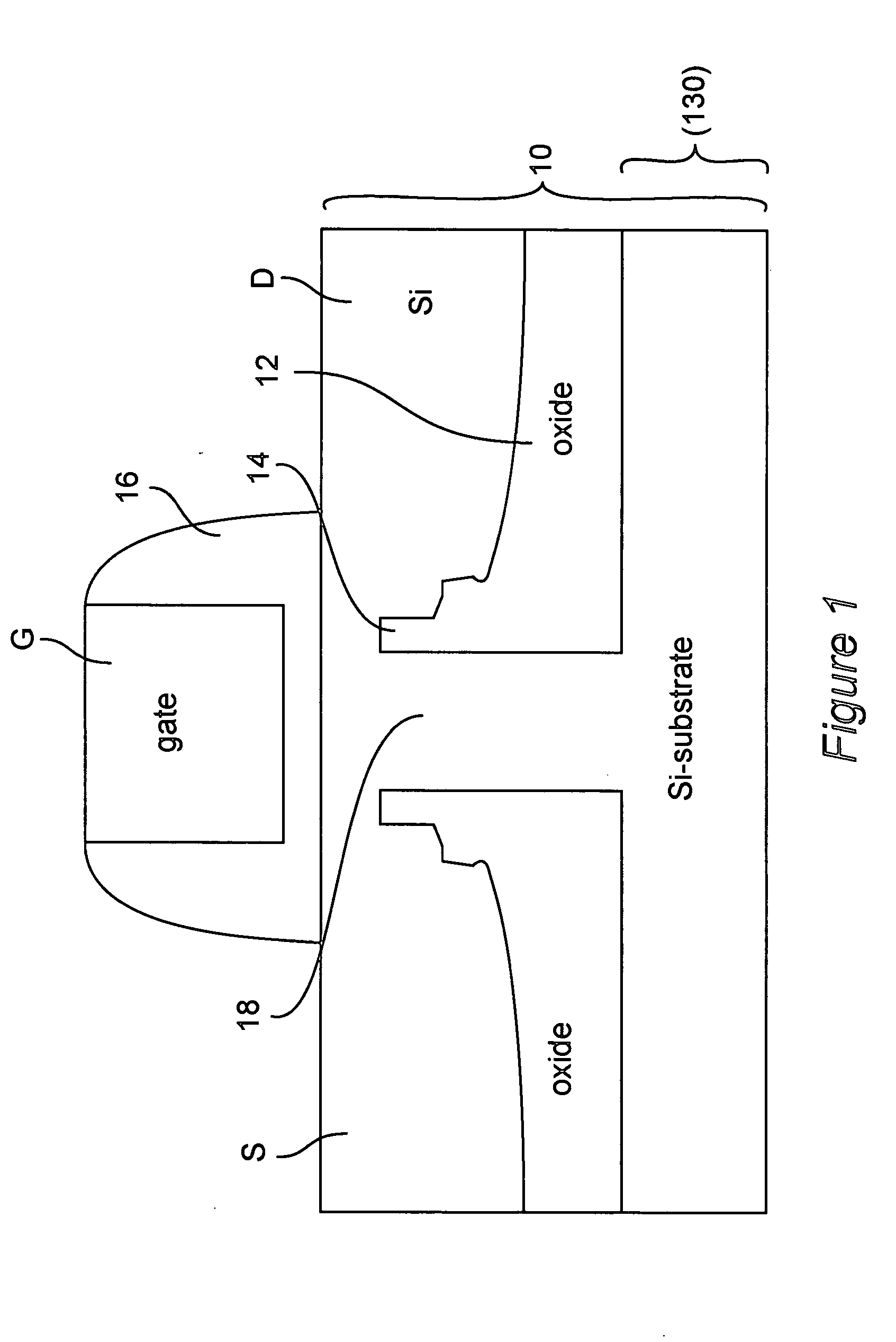
[0028] Referring now to FIG. 9 a generalized cross-sectional view of a second preferred embodiment for applying stresses within the substrate or layer of semiconductor material is shown. It may be helpful to an appreciation of the scope of the present invention to compare FIG. 9 with FIG. 1, discussed above. In particular, the second preferred embodiment provides a discontinuous insulator film structure within a portion of a substrate underlying a transistor and having discontinuies aligned (e.g. self-aligned) with the gate thereof and lying below the conduction channel of the transistor. However, the discontinuous film is a stressed film aligned with and underlying the gate structure rather than having an aperture aligned with the gate and a second stressed insulator film is also preferably included to enhance the effects of the first film in providing further increased stress in the channel. It will also be observed by those skilled in the art that FIG. 9 illustrates a transistor ...
second embodiment
[0037] Referring now to FIG. 25A, a thin oxide 270 is deposited to protect the surface under the channel and then a tensile nitride film 280 is deposited to add additional compressive stress to the channel. This stress is efficiently transferred to the channel since the film thus substantially surrounds the transistor both above and below the channel (e.g. but for STI structure 225 which could optionally be opened and stressed film applied therein to even more fully surround the transistor). The thickness of layer 280 may be designed to regulate the amount of stress applied. Those skilled in the art will also appreciate that this configuration of the stress film 280 can apply additional stress beyond the stress which can be applied in shear from a planar or conformal layer as in the second embodiment described above or previously proposed surface applications of the stressed film within the adhesion limits of the film. Further, since the stressed film substantially surrounds the tra...
third embodiment
[0039] The comparative meritorious effects of these variant forms of the invention are graphically illustrated in FIG. 26. FIG. 26, for clarity, shows only compressive stress along the 10 nm thickness of the channel at 5 nm below the gate oxide after etch of the strained SiGe (solid line 310) and after deposit of 40 nm of stressed nitride (dashed line 320) in which the stress was about 1.5 GPa. The removal of the strained SiGe under the gate produces about 600 MPa of stress in the channel with substantial peaks proximate to the source and drain junctions (as in SON devices) and a substantial contribution and increase of that stress is also clearly attributable to further stressed film deposits (as in SOI and bulk semiconductor devices).
[0040] In view of the foregoing, it is seen that the invention provides a structure within a semiconductor substrate or layer and a reliable technique for forming such a structure which has substantial and varied meritorious effects or transistor perf...
PUM
 Abstract
Description
Claims
Application Information