Method for fabricating strained silicon-on-insulator structures and strained silicon-on insulator structures formed thereby

a technology of strained silicon and strained silicon, which is applied in the direction of semiconductor devices, electrical devices, transistors, etc., can solve the problems of poor thermal conductivity of silicon germanium layers, inability to optimize nfet's and pfet's separately, and the global silicon germanium layers deposited across the wafer are not suitable for optimizing nfet's and pfet's. achieve the effect of improving the device performance and enhancing carrier mobility

Active Publication Date: 2005-10-13
GLOBALFOUNDRIES US INC
View PDF29 Cites 92 Cited by
  • Summary
  • Abstract
  • Description
  • Claims
  • Application Information

AI Technical Summary

Benefits of technology

[0009] In accordance with the principles of the invention, locally increasing the thickness of the buried insulating layer transfers tensile stress locally to the overlying active layer. Regions of the active layer, which are defined by an oxidation mask, are strained by the tensile stress. The strained active layer is characterized by an enhanced carrier mobility, thereby improving the device

Problems solved by technology

Silicon germanium layers tend to introduce defects in the silicon that impact device yields.
Global silicon germanium layers deposited across the wafer are not suitable for separately optimizing NFET's and PFET's.
Silicon germanium layers also have poor thermal conductivity and some dopants diffuse more rapidly through t

Method used


Image

  • Method for fabricating strained silicon-on-insulator structures and strained silicon-on insulator structures formed thereby
  • Method for fabricating strained silicon-on-insulator structures and strained silicon-on insulator structures formed thereby
  • Method for fabricating strained silicon-on-insulator structures and strained silicon-on insulator structures formed thereby

Examples


Embodiment Construction

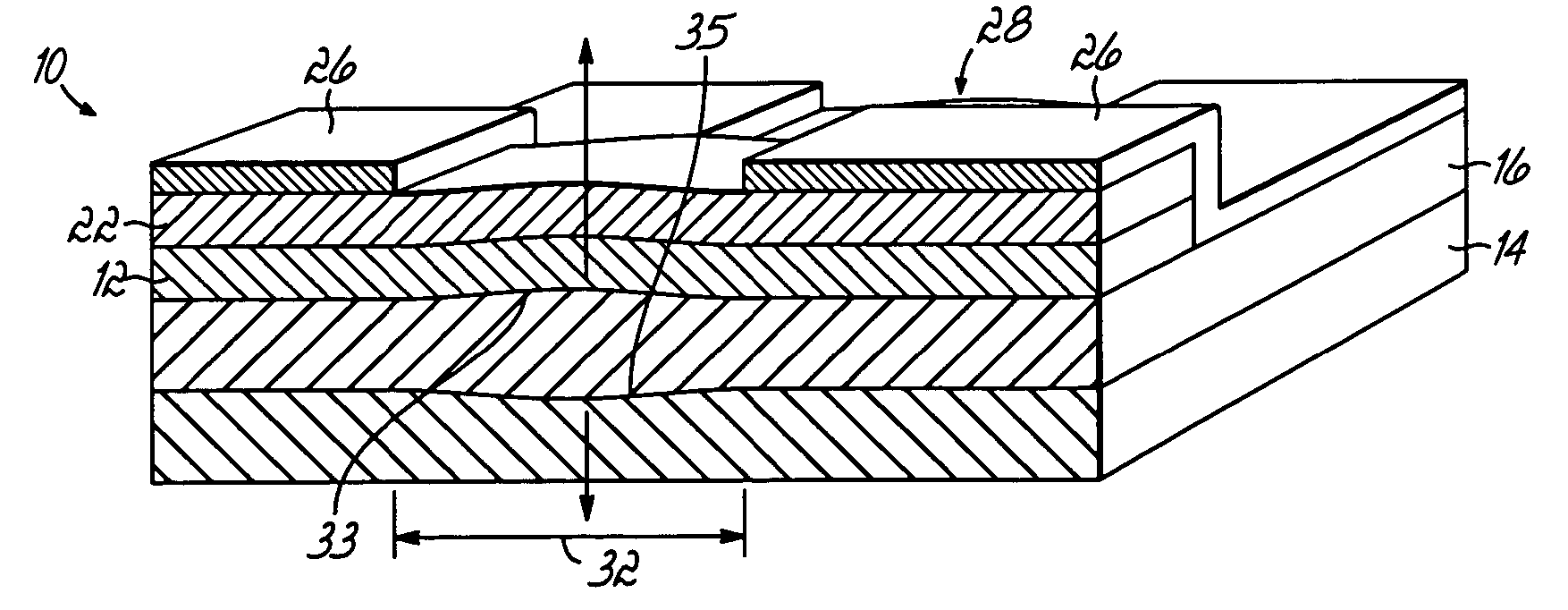
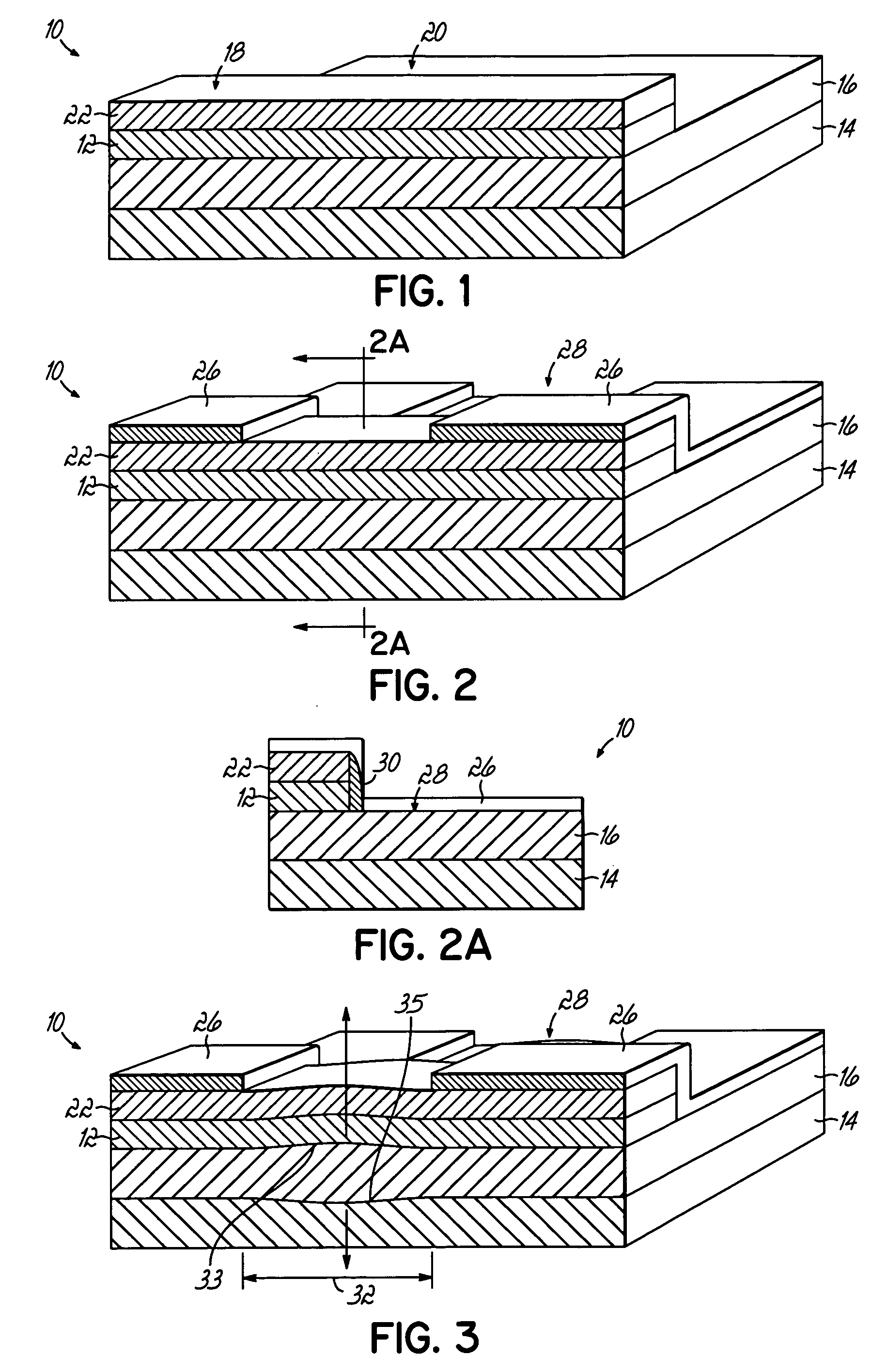
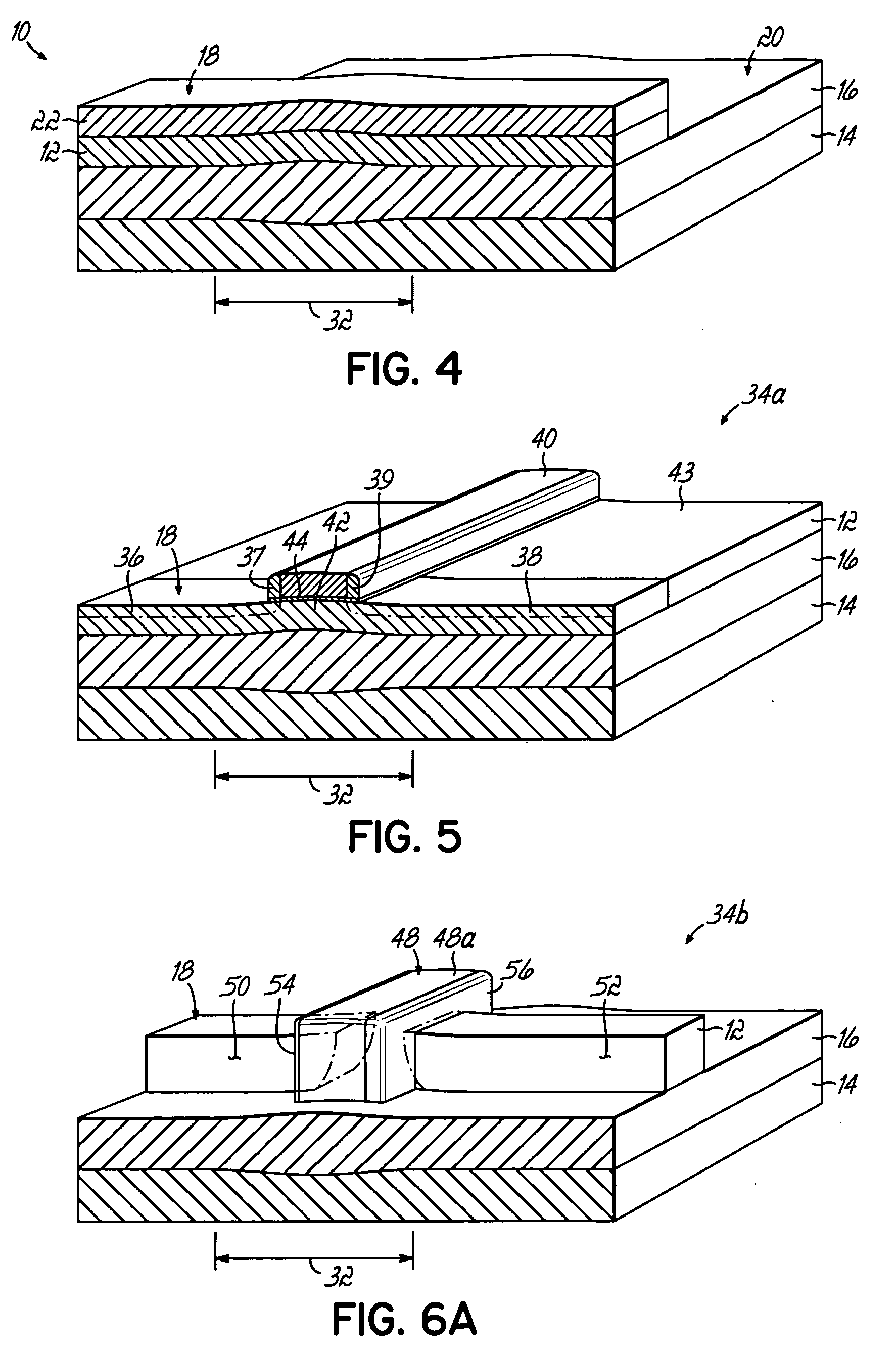
[0020] With reference to FIG. 1, a silicon-on-insulator (SOI) substrate 10 includes an active layer 12 of silicon, or another suitable semiconductor material, separated vertically from a handle wafer 14 by an insulating layer 16. Insulating layer 16 electrically isolates the active layer 12 from the handle wafer 14. The SOI substrate 10 may be fabricated by any standard technique, such as wafer bonding or a separation by implantation of oxygen (SIMOX) technique. In the illustrated embodiment of the invention, the silicon constituting the active layer 12 may be doped initially with an n-type dopant to render it n-type or a p-type dopant to render it p-type. The handle wafer 14 may be formed from any suitable semiconductor material including, but not limited to, silicon and polycrystalline silicon (polysilicon). The dielectric material constituting insulating layer 16 is typically silicon dioxide having a thickness in the range of about fifty (50) nanometers to about 150 nanometers, b...


PUM


Abstract

A silicon-on-insulator (SOI) device and structure having locally strained regions in the silicon active layer formed by increasing the thickness of underlying regions of a buried insulating layer separating the silicon active layer from the substrate. The stress transferred from the underlying thickened regions of the insulating layer to the overlying strained regions increases carrier mobility in these confined regions of the active layer. Devices formed in and on the silicon active layer may benefit from the increased carrier mobility in the spaced-apart strained regions.

Description

FIELD OF THE INVENTION [0001] The invention relates generally to semiconductor structures and devices and to a method for their fabrication and, more particularly, to fabrication methods and silicon-on-insulator (SOI) structures, devices and integrated circuits characterized by enhanced carrier mobility. BACKGROUND OF THE INVENTION [0002] Silicon-on-insulator (SOI) structures are constituted by a thin active silicon layer overlying a silicon dioxide insulating layer (i.e., the buried oxide, or “BOX”), which itself overlies a supporting silicon substrate. The advantages of SOI structures for metal-oxide-semiconductor field effect transistor (MOSFET) technology and complimentary metal-oxide-semiconductor (CMOS) integrated circuits are well documented. The insulating layer of the SOI structure enables field effect transistors (FET's) to operate at significantly higher speeds with improved electrical isolation and reduced electrical losses as compared with conventional bulk silicon tech...

Claims


Application Information

Patent Timeline
IPC IPC(8): H01L21/336H01L21/762H01L21/84H01L27/12H01L29/786
CPCH01L21/7624H01L29/66772H01L29/66795H01L29/7842H01L29/78654H01L29/785H01L29/78603H01L29/78645H01L29/7849H01L21/20H01L21/84
Inventor FURUKAWA, TOSHIHARUKOBURGER, CHARLES WILLIAM IIISLINKMAN, JAMES ALBERT
Owner GLOBALFOUNDRIES US INC
Why Eureka
Try Eureka