Method for making a five square vertical DRAM cell
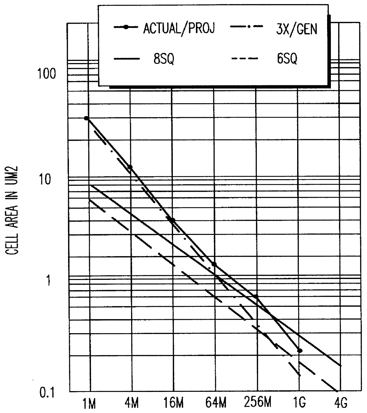
a vertical dram cell and dram technology, applied in the field of computer chip manufacture, can solve the problems of linear cell nature, too large 8-square cell to meet density, too large to fit on a standard package,
- Summary
- Abstract
- Description
- Claims
- Application Information
AI Technical Summary
Problems solved by technology
Method used
Image
Examples
Embodiment Construction
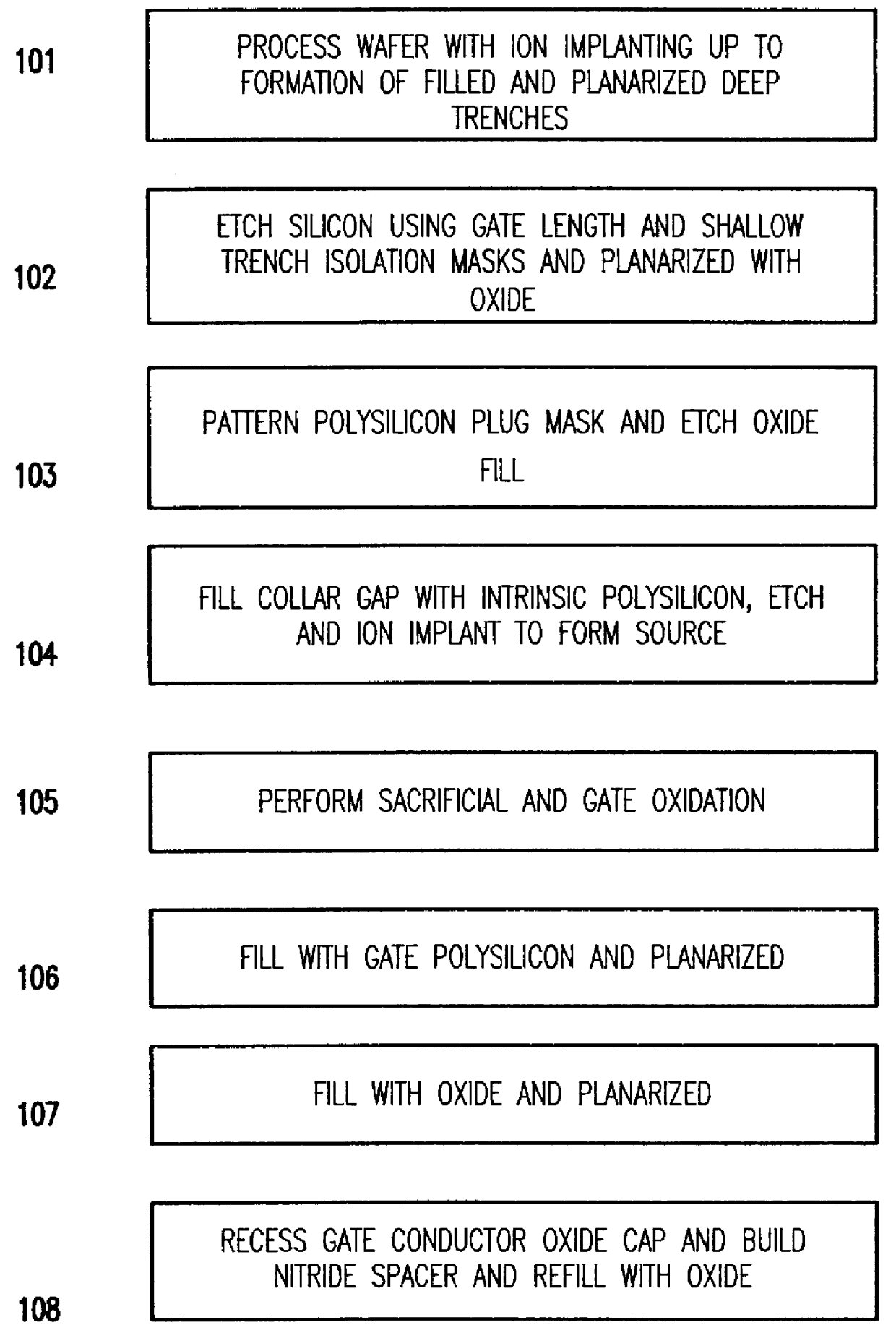
Referring now to the drawings, and more particularly to FIG. 3, there is shown a flow chart of the process sequence of the present invention.
As can be seen from the step shown in block 101, the process begins with a wafer which is similar to wafers used in Merged Isolation Node Trench (MINT) processing as described in U.S. Pat. No. 4,801,988 to Kenney, which is herein incorporated by reference. In the initial steps the inventive process varies by adding arsenic implantation and out diffusion steps. Start with a wafer with a top thickness of -1 .mu.m doped to the concentration of the vertical device channel. Follow with a bit line drain ion implant (arsenic) to form the top part of the device. Then, as in MINT processing, a quick oxidation, a thin nitride layer and TEOS are formed on the substrate. Then, a deep trench is formed and arsenic is out diffused to form the buried plate. Then, as in MINT processing, a thin insulating layer lines the trench. The trench is filled with polysil...
PUM
 Abstract
Description
Claims
Application Information


