Semiconductor device and method of manufacturing same

Inactive Publication Date: 2000-08-22
DENSO CORP
View PDF13 Cites 39 Cited by
  • Summary
  • Abstract
  • Description
  • Claims
  • Application Information

AI Technical Summary

Problems solved by technology

That is to say, if the concave configuration, the side surface of which becomes the channel part, is formed by LOCOS technique alone, the LOCOS oxidation time period would lengthen, and the angle of the groove side surface would be as gentle as approximately 30.degree., which would make it impossible t

Method used


Image

  • Semiconductor device and method of manufacturing same
  • Semiconductor device and method of manufacturing same
  • Semiconductor device and method of manufacturing same

Examples


first embodiment

the present invention will now be described with reference to the accompanying drawings.

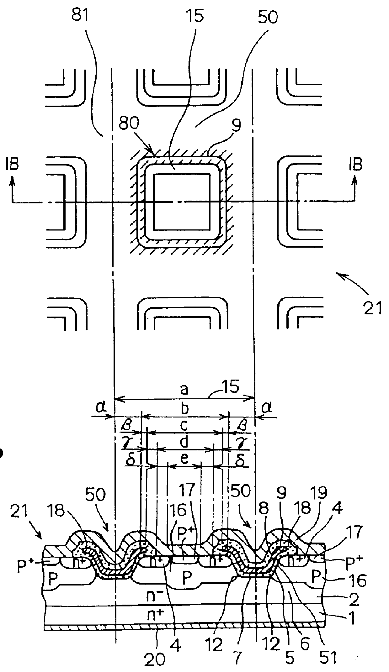
FIG. 1A is a plan view of a vertical type power MOSFET composed of numerous square unit cells according to the present invention, and FIG. 1B is a cross-sectional view taken along line IB--IB of FIG. 1A. FIGS. 2 through 21 are descriptive views of the respective stages of the manufacturing method for the vertical type power MOSFET.

The main part (unit cell part) of the vertical type power MOSFET according to this embodiment is so constructed (i.e., a lattice pattern) as illustrated in FIGS. 1A and 1B in which numerous unit cells 15 are laid out lengthwise and breadthwise at a pitch (unit cell dimension) of a.

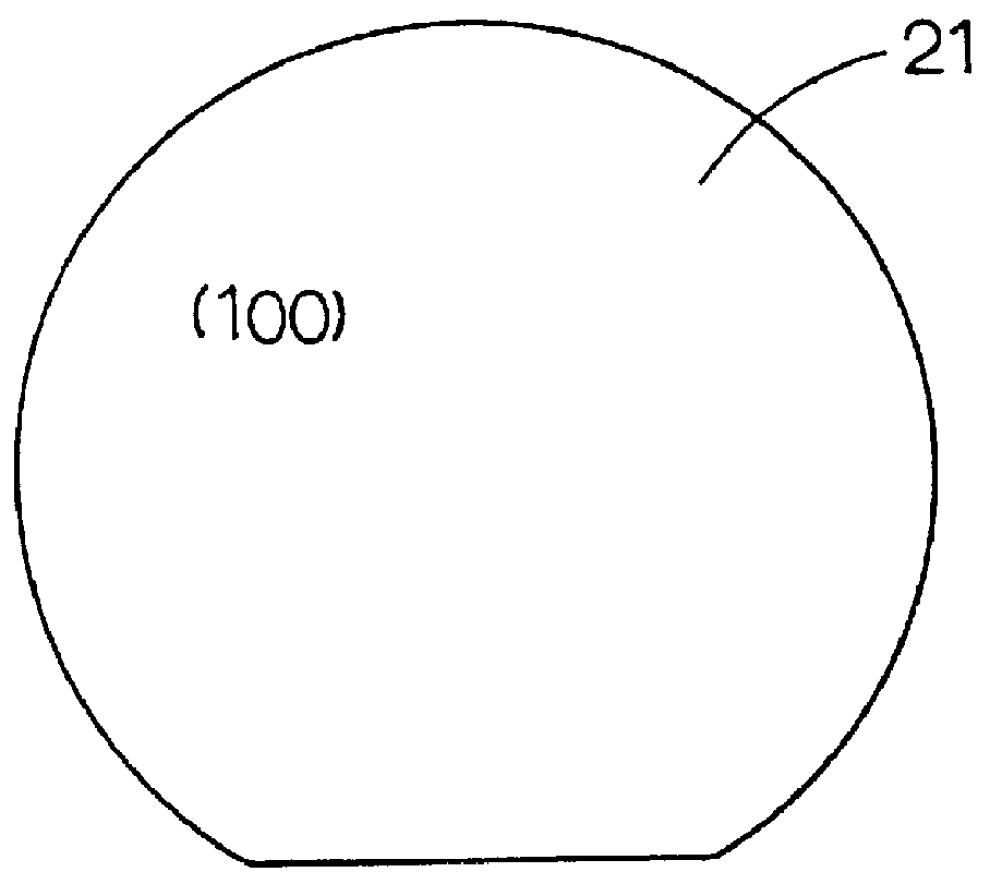
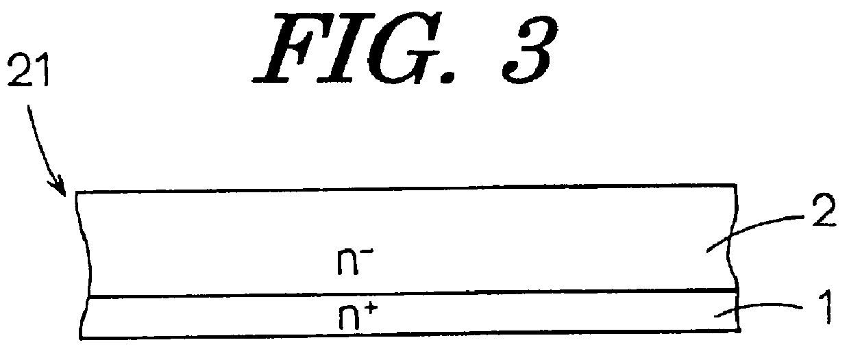
In FIG. 1A, a wafer 21 is composed of a semiconductor substrate 1 comprising an n.sup.+ -type silicon to an impurity concentration of about 10.sup.19 .about.10.sup.20 cm.sup.-3 and a thickness of 100-300 .mu.m and an n.sup.- -type epitaxial layer 2 formed to an impurity concentration of about ...


PUM


Abstract

A concave channel type DMOS structure having an improved gate-to-source breakdown voltage are disclosed. By establishing a curvature at a corner portion of a lattice-like pattern in a groove portion for forming the concave channel structure, the shape of the tip of a three-dimensionally projecting portion of a semiconductor region determined by a plane angle of the corner portion in the lattice-like pattern and an inclination of the groove portion is rounded. That is, a three-dimensionally sharpened corner portion in the concave channel structure is rounded, and thereby electric field concentration at the corner portion is suppressed.

Description

This application is based upon and claims the benefit of priority of the prior Japanese Patent Application Nos. (Hei) 7-253747 filed on Sep. 29, 1995 and (Hei) 7-253748 filed on Sep. 29, 1995, incorporated herein by reference.1. Field of the InventionThe present invention relates to a semiconductor device suitably employed for a MOS-IC etc. as a single unit or with the incorporation of a power semiconductor device.2. Related ArtsRecently, a vertical type power MOSFET has been used in many industrial fields for various features thereof such as high frequency characteristics, fast switching speed and low power driving.As a conventional vertical type power MOSFET, there have been disclosed concave channel type DMOS structures in International Publication No. PCT WO93 / 03502 and the Japanese Unexamined Patent Publication No. 62-12167, for example. The proposed DMOS structure has a concave structure or a bathtub-shaped groove structure fabricated by a combination of local oxidation of sil...

Claims


Application Information

Patent Timeline
IPC IPC(8): H01L21/02H01L29/06H01L29/66H01L29/739H01L21/336H01L29/02H01L29/78
CPCH01L29/0696H01L29/7397H01L29/7813H01L29/7398H01L29/7809
Inventor OKABE, NAOTOYAMAMOTO, TSUYOSHI
Owner DENSO CORP
Why Eureka
Try Eureka